Light emitting device using fluorescent substance

a technology fluorescent substance, which is applied in the direction of discharge tube luminescent screen, discharge tube/lamp details, discharge tube luminescent composition, etc., can solve the problems of spoiled reliability of light emitting device, and achieve the effects of good color rendering properties, extremely small deterioration of output power and color shi

Inactive Publication Date: 2005-08-18
NICHIA CORP
View PDF9 Cites 43 Cited by
  • Summary
  • Abstract
  • Description
  • Claims
  • Application Information

AI Technical Summary

Benefits of technology

[0012] Accordingly, an object of the present invention is to provide a light emitting device in which det

Problems solved by technology

However, to utilize the light emitting devise with the advantages of semiconductor light emitting element as a light source such as a lighting, current light emitting devices are not enough, so improvement in the brightness and improvement in the productivity are required.
Furth

Method used


Image

  • Light emitting device using fluorescent substance
  • Light emitting device using fluorescent substance
  • Light emitting device using fluorescent substance

Examples


example 1

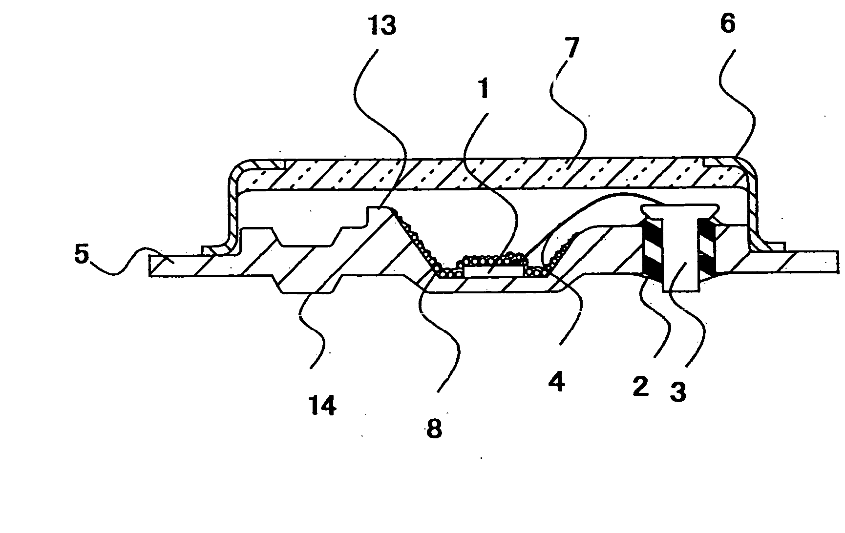
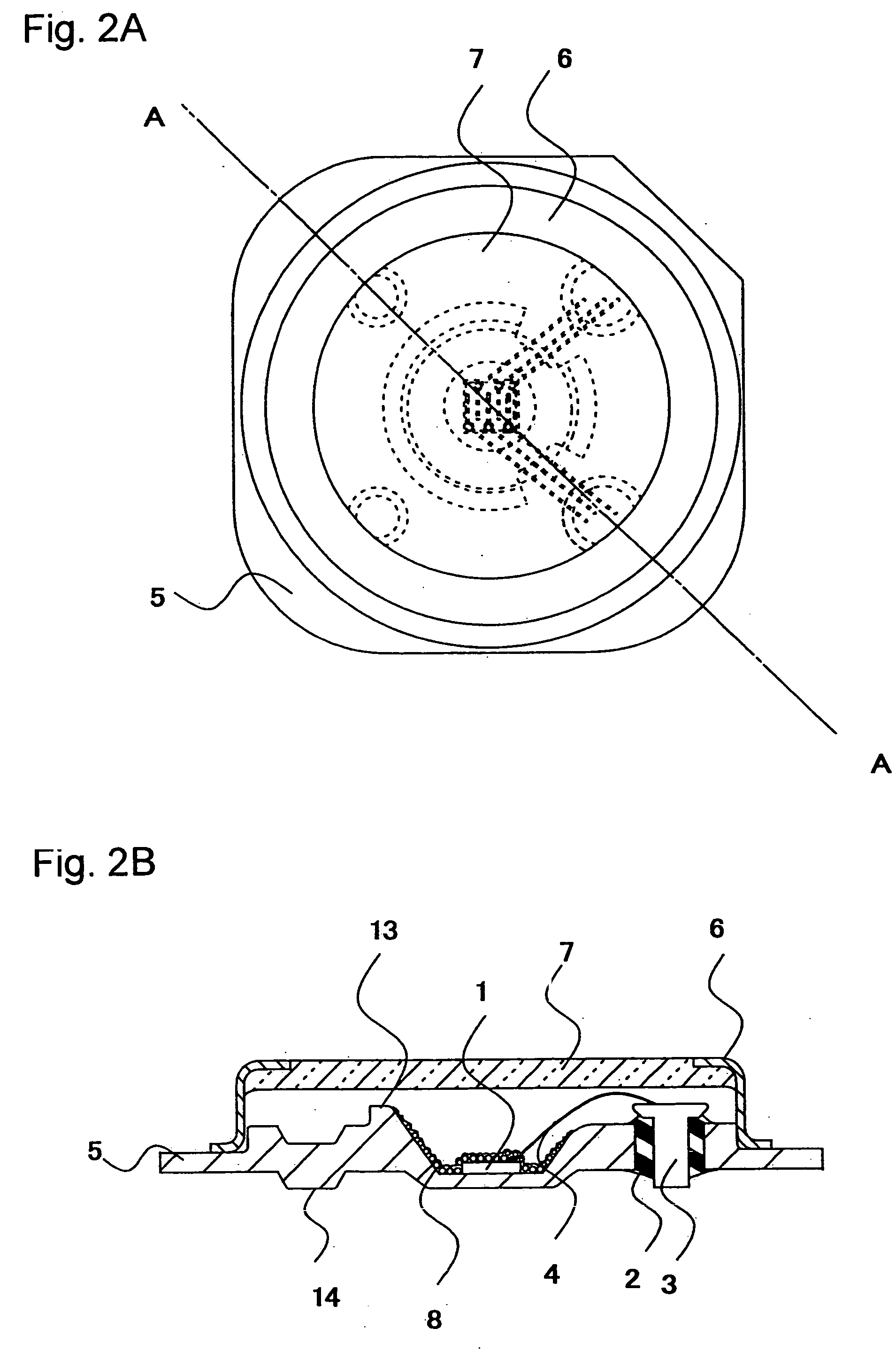
[0101] The light emitting device of surface mounting type shown in FIG. 2 is made. The LED chip 1 is a nitride semiconductor element having a light emitting layer made of InAlGaN semiconductor of which peak wavelength is 400 nm of ultraviolet.

[0102] More concretely, the LED chip 1 can be formed by depositing the nitride semiconductors on a washed sapphire substrate by MOCVD method using TMG(trimethyl-gallium) gas, TMI(trimethyl-indium) gas, nitrogen gas and dopant gas together with carrier gas. A layer to be the n-type nitride semiconductor and A layer to be the p-type nitride semiconductor can be made by changing between SiH4 and Cp2Mg as a dopant gas.

[0103] The LED chip 1 has a element structure constituted by laminating an n-type GaN layer of undoped nitride semiconductor, an Si doped GaN layer which is n-type contact layer to be formed with an n-type electrode, an n-type GaN layer of undoped nitride semiconductor, an AlGaN layer including Si which is n-type cladding layer and ...

example 2

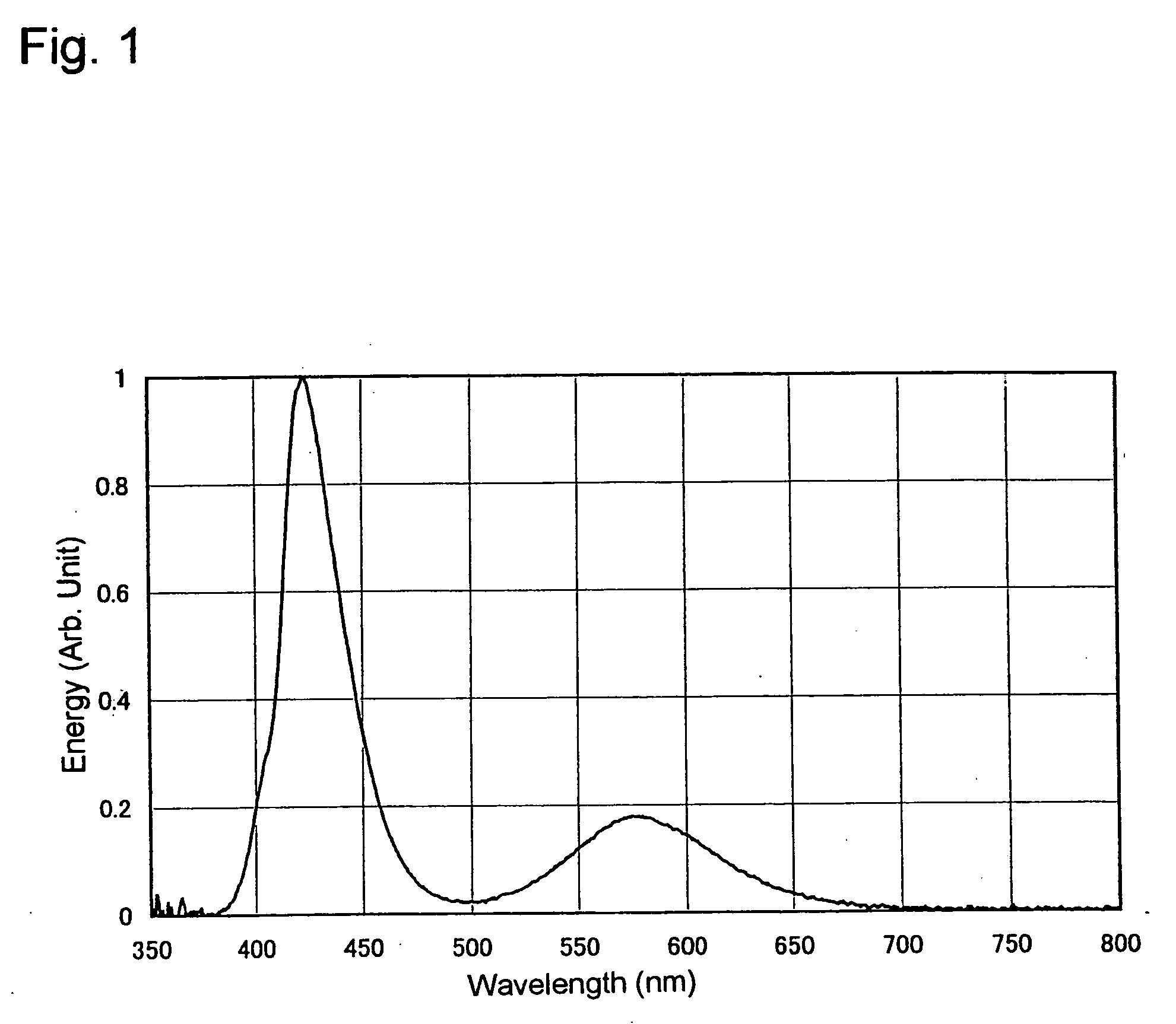
[0119] The light emitting device is made similar to Example 1 except that the raw materials of SrCO3, MnCO3 and Eu2O3 are adjusted and mixed according to the composition ratio (Sr0.94, Eu0.05, Mn0.01)2B5O9Cl by changing the ratio in the phosphor of Example 1, thereby obtaining the color tone of the chromaticity coordinates (x,y)=(0.210,0.103). Moreover, the luminous efficiency is 23.9 lm / W at the drive condition of 20 mA. If the luminescent brightness of comparative example 1 is regarded as 100%, the luminescent brightness is about 206% in the light emitting device excited by 400 nm according to Example 2. In the light emitting device excited by 365 nm, the chromaticity coordinates (x,y)=(0.211,0.105) can be obtained and the luminescent brightness is about 139%.

example 3

[0120] The light emitting device is made similar to Example 1 except that the raw materials of SrCO3, MnCO3 and Eu2O3 are adjusted and mixed according to the composition ratio of (Sr0.92, Eu0.05, Mn0.03)2B5O9Cl by changing the ratio in the phosphor of Example 1, thereby obtaining the color tone of the chromaticity coordinates(x,y)=(0.284,0.210) can be obtained. Moreover, the luminous efficiency is 24.7 lm / W at the drive condition of 20 mA. If the luminescent brightness of comparative example 1 is regarded as 100%, the luminescent brightness is about 213% in the light emitting device excited by 400 nm according to Example 2. In the light emitting device excited by 365 nm, the chromaticity coordinates(x,y)=(0.285,0.212) can be obtained and the luminescent brightness is about 144%.


PUM


Abstract

A light emitting device related to the present invention, which has a semiconductor light emitting element and a phosphor which converts a part of the luminescence spectrum emitted from the semiconductor light emitting element, characterized in that the luminescence spectrum of the semiconductor light emitting element is located between a near ultraviolet region and a short-wavelength visible region, and the phosphor is made by adding a red luminescent activator to a base material of a blue luminescent phosphor, thereby improving the color shading generated by the dispersion of the spectra of the light emitting elements and obtaining the light emitting device having a high brightness and a good color rendering properties. With this, it is possible to provide the light sources for the lighting apparatus of medical treatments, the flash plate of a copying machine, etc., in which a good color rendering property is required.

Description

TECHNICAL FIELD [0001] The invention is related to a light emitting device having a light emitting element and a phosphor, which can be used for various light sources such as a signal light, lighting, a display, an indicator. Especially, the present invention provides the light emitting device which can emit a white light by using the phosphor which is excited by the emission spectrum from the light emitting element and capable of emitting a visible light. BACKGROUND ART [0002] Various light emitting diodes and laser diodes are developed as a semiconductor light emitting device today. Such a semiconductor light emitting device has began to substitute for an electric bulb and a cold cathode tube as various light sources, such as a display, a back light and an indicator by using the strong points of a low-voltage drive, small sizing, lightweight, thin shape, high reliability with a long-life, low electrical power consumption. [0003] Especially, the light emitting element using the nit...

Claims


Application Information

Patent Timeline
IPC IPC(8): C09K11/08H01L33/06C09K11/77H01L33/32H01L33/50H01L33/62H05B33/14
CPCC09K11/0883C09K11/7734C09K11/7739H05B33/14C09K11/7789H01L33/502H01L33/504C09K11/774H01L2224/48091H01L2224/8592H01L2224/45139H01L2924/00014H01L2924/00H01L2224/45015H01L2924/207
Inventor MURAZAKI, YOSHINORI
Owner NICHIA CORP
Why Eureka
Try Eureka