System and method for fabricating diodes

a diode and diode technology, applied in the field of system and method for fabricating diodes, can solve the problems of preventing the commercialization of semiconductors, affecting the manufacturing of semiconductor/solid-state devices, and exhibiting a constant forward current density degraded forward voltage drop in current technology of sic pin and pn diodes

Inactive Publication Date: 2005-08-25
SUDARSHAN T S +2
View PDF7 Cites 12 Cited by
  • Summary
  • Abstract
  • Description
  • Claims
  • Application Information

AI Technical Summary

Problems solved by technology

However, the current technology of SiC PiN and PN diodes consistently exhibit a degraded forward voltage drop under constant forward current density during use.
This disadvantage of the present state of the art of SiC diodes has prevented their commercialization.
The disadvantages of SiC semiconductors is primarily related to material defects, particularly in the epitaxial layer of SiC diodes.
Such defects behave as a deep energy level that traps carriers in the drift region of the diode, thereby reducing the carrier lifetime and increasing the forward voltage drop.
The main obstacle in the fabrication of high power SiC PN and PiN junction diodes is the existence of defects that cause forward voltage drop degradation with time (voltage drift).
This disadvantage is observed in diodes formed by both ion implantation and epitaxial growth.
Stacking faults prevent the realization of long-term reliable SiC diodes.
Thus far, no system or method for eliminating forward voltage drift in SiC diodes that have low forward voltage drops has been provided.
Degradation of forward voltage drop in SiC diodes destroys the usability of diodes.
Such quick failure has prevented the wide-spread commercialization of SiC diodes.
However, an increase in the doping concentration can result in increase of mismatch stresses.
If the mismatch stresses exceed the value of critical shear stress, crystal lattice defects such as dislocations are formed.
The formed dislocations act as nucleation sites for the generation of stacking faults, and can be responsible for the degradation of SiC diode and result in disadvantageous forward current-voltage characteristics.
Conventional methods, such as ion implantation and epitaxial growth used to form PN junctions in SiC devices, generally, result in the formation of abrupt PIN junctions.
If the value of the stresses exceeds the yield stress (˜1 MPa for SiC), mismatch dislocations might be generated.
These broken bonds can be carrier traps, which might result in an increase of the series resistance during PiN diode operation and, hence, in forward voltage drop increase.

Method used


Image

  • System and method for fabricating diodes
  • System and method for fabricating diodes
  • System and method for fabricating diodes

Examples


Embodiment Construction

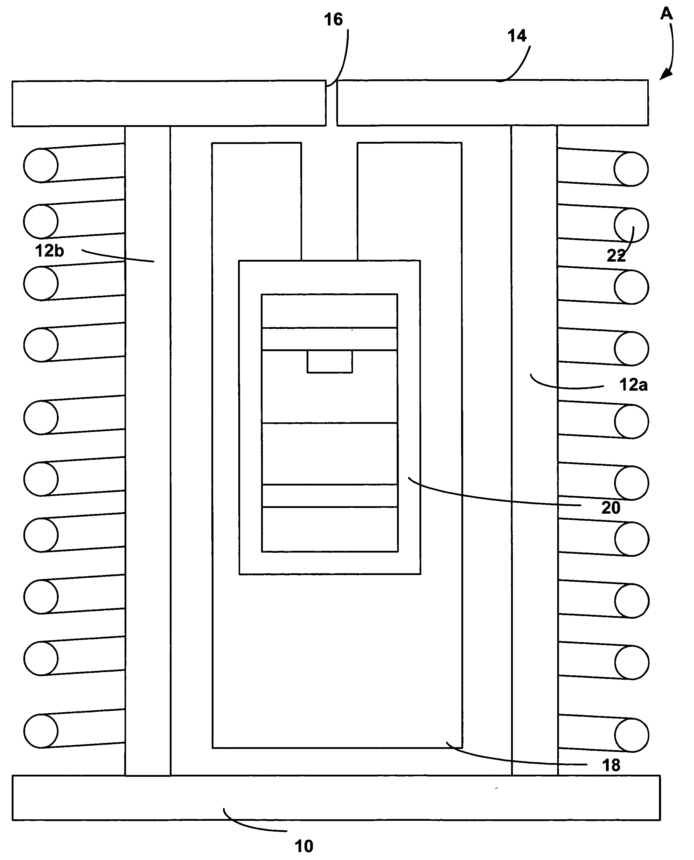
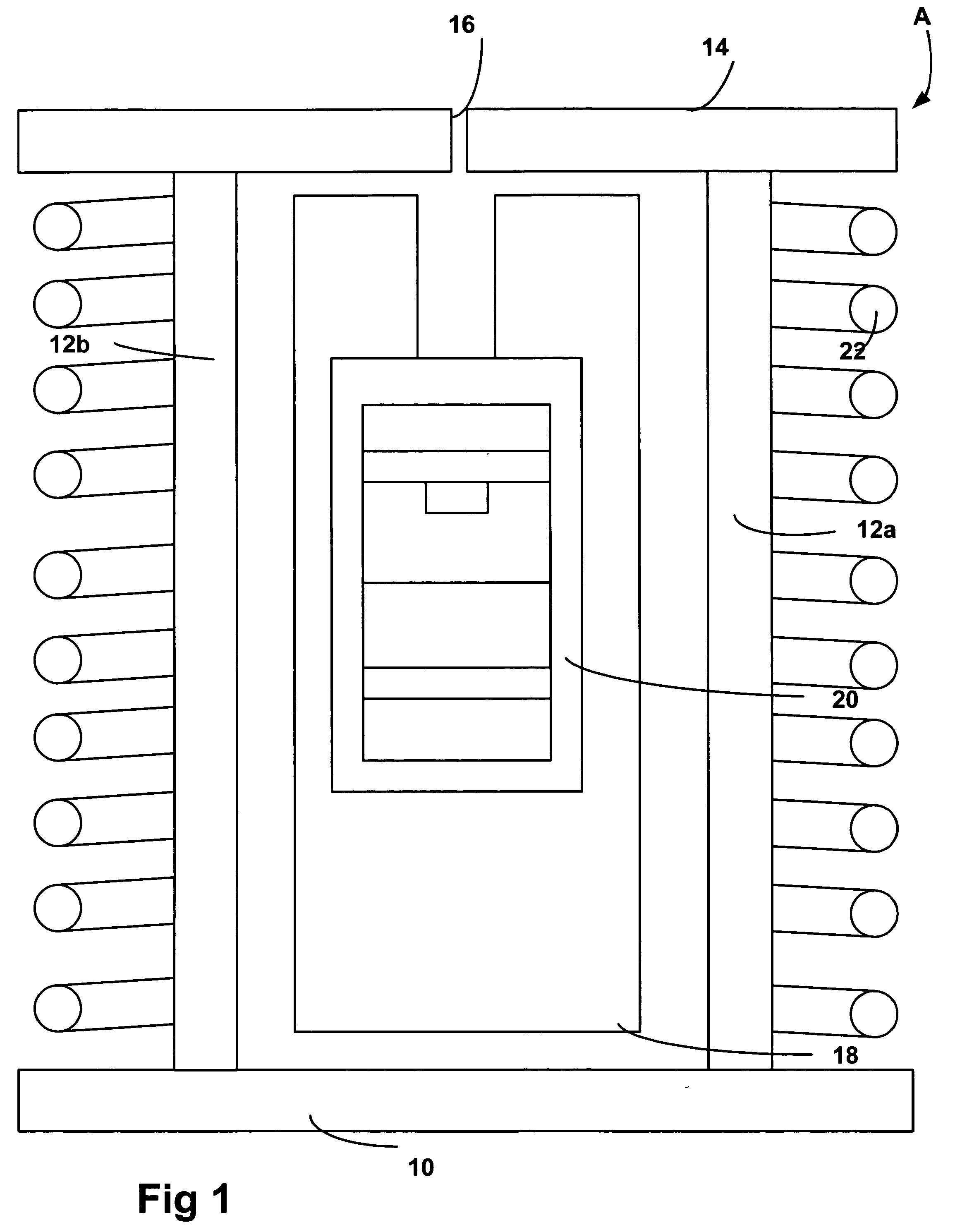
[0038] This invention is a novel system and method for PN and PiN diode fabrication, that results in operation of the diodes without voltage drift. This new process involves the formation of a graded, deep pn junction resulting from diffusion of acceptor impurity into a substrate, particularly a SiC substrate. It is advantageous to form a deep and graded doping concentration profile in the pn junction region to avoid the degradation of forward voltage drop. Deep pn junctions are advantageous to make sure that the pn junction is of sufficient distance from the near-surface p+ region to prevent adverse effects from any generation of structural defects. For example, when the p+ layer is Aluminum-doped, the effect of generated defects on the diode performance is not significant since the pn junction is located much deeper than the p+ Al surface layer.

[0039] By using diffusion, an acceptor impurity atom, such as Boron, penetrates much deeper into the substrate and forms a graded concent...


PUM

PropertyMeasurementUnit
pressureaaaaaaaaaa
thicknessaaaaaaaaaa
pressureaaaaaaaaaa

Abstract

This invention is directed to a system and method of fabricating PN and PiN diodes by diffusing an acceptor impurity into a substrate. This invention is particularly advantageous for fabricating SiC diodes having linearly graded, deep pn junctions. One method that this invention uses to achieve its advantages is by diffusing an acceptor impurity into a substrate using a crucible, acceptor source, substrate, and furnace.

Description

CROSS-REFERENCE TO RELATED APPLICATION [0001] This application is a divisional application of nonprovisional application Ser. No. 10 / 837,862 entitled A System and Method for Fabricating Diodes, filed May 3, 2004, which in turn claims priority on provisional patent application No. 60 / 519,248, entitled A Method For Eliminating Forward Voltage Drift in Diodes, filed Nov. 12, 2003, and provisional patent application No. 60 / 466,961, entitled A Method For Eliminating Forward Voltage Drift in Diodes, filed May 1, 2003.FIELD OF THE INVENTION [0002] This invention is directed to a system and method for fabricating diodes and particularly to a system and method for fabricating a SiC diode. BACKGROUND OF THE INVENTION [0003] Silicon Carbide (SiC) has been recognized as the next generation semiconductor material to replace Si for high power and high frequency applications, particularly, under extreme conditions, such as high temperature and high radiation (e.g. in the space and nuclear reactors...

Claims


Application Information

Patent Timeline
Patent Type & Authority Applications(United States)
IPC IPC(8): H01LH01L29/15H01L29/22H01L29/24H01L31/0312H01L31/105
CPCH01L21/0455H01L29/1608Y10S438/931H01L29/861H01L29/6606
Inventor SUDARSHAN, T.S.SOLOVIEV, STANISLAVGAO, YING
Owner SUDARSHAN T S
Why Eureka
Try Eureka