
Integrated circuit with enhancement mode pseudomorphic high electron mobility transistors having on-chip electrostatic discharge protection

a high electron mobility, transistor technology, applied in transistors, electrical devices, semiconductor devices, etc., can solve the problems of inability to use large on-chip esd protection devices, etc., to increase gate-to-drain, high electron mobility transistors, and reduce chip area occupied

Inactive Publication Date: 2005-09-01
AVAGO TECH WIRELESS IP SINGAPORE PTE
View PDF6 Cites 17 Cited by
  • Summary
  • Abstract
  • Description
  • Claims
  • Application Information

AI Technical Summary

Benefits of technology

[0004] An integrated circuit (IC) with high electron mobility transistors, such as enhancement mode pseudomorphic high electron mobility transistors (E-pHEMTs) and method for fabricating the IC utilizes an increased gate-to-drain etch recess spacing in some of the high electron mobility transistors to provide on-chip electrostatic discharge (ESD) protection. The use of the increased gate-to-drain etch recess spacing allows smaller high electron mobility transistors to be used for ancillary low speed applications on the IC, which reduces the chip area occupied by these ancillary transistors.
[0006] A method for fabricating an integrated circuit with at least one high electron mobility transistor includes proving a substrate, and forming a high electron mobility transistor with a source electrode, a drain electrode and a gate electrode on the substrate. The forming of the high electron mobility transistor includes creating an increased gate-to-drain etch recess spacing. The increased gate-to-drain etch recess spacing provides a greater protection for the high electron mobility transistor from an ESD on the drain electrode.

Problems solved by technology

However, due to the high costs associated with the manufacturing of RFICs with E-pHEMTs, the use of large on-chip ESD protection devices in the RFICs is not practical.
Even if manufacturing costs are ignored, the demand for smaller RFICs prohibits the use of large on-chip ESD protection devices.

Method used


Image

  • Integrated circuit with enhancement mode pseudomorphic high electron mobility transistors having on-chip electrostatic discharge protection
  • Integrated circuit with enhancement mode pseudomorphic high electron mobility transistors having on-chip electrostatic discharge protection
  • Integrated circuit with enhancement mode pseudomorphic high electron mobility transistors having on-chip electrostatic discharge protection

Examples


Embodiment Construction

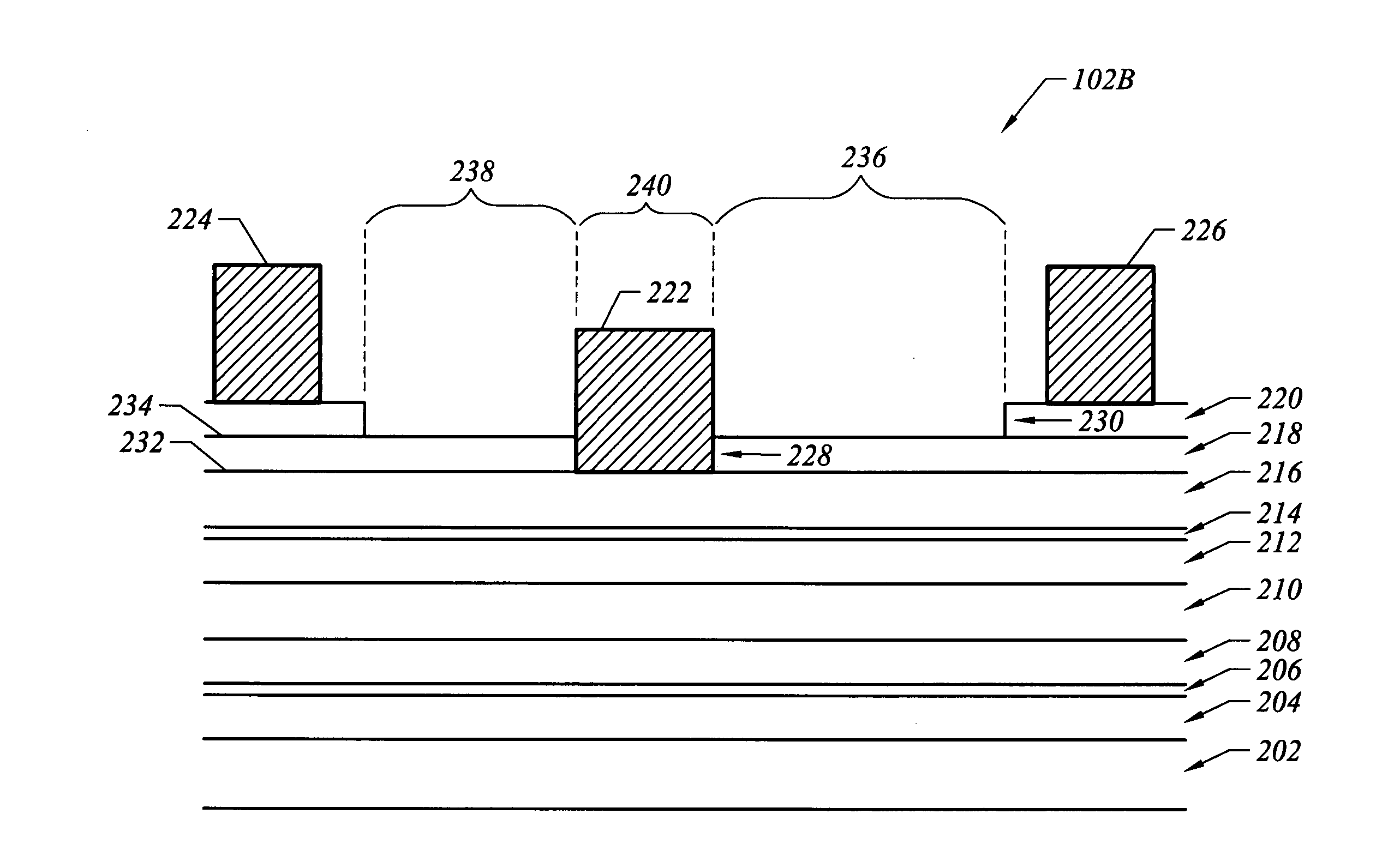
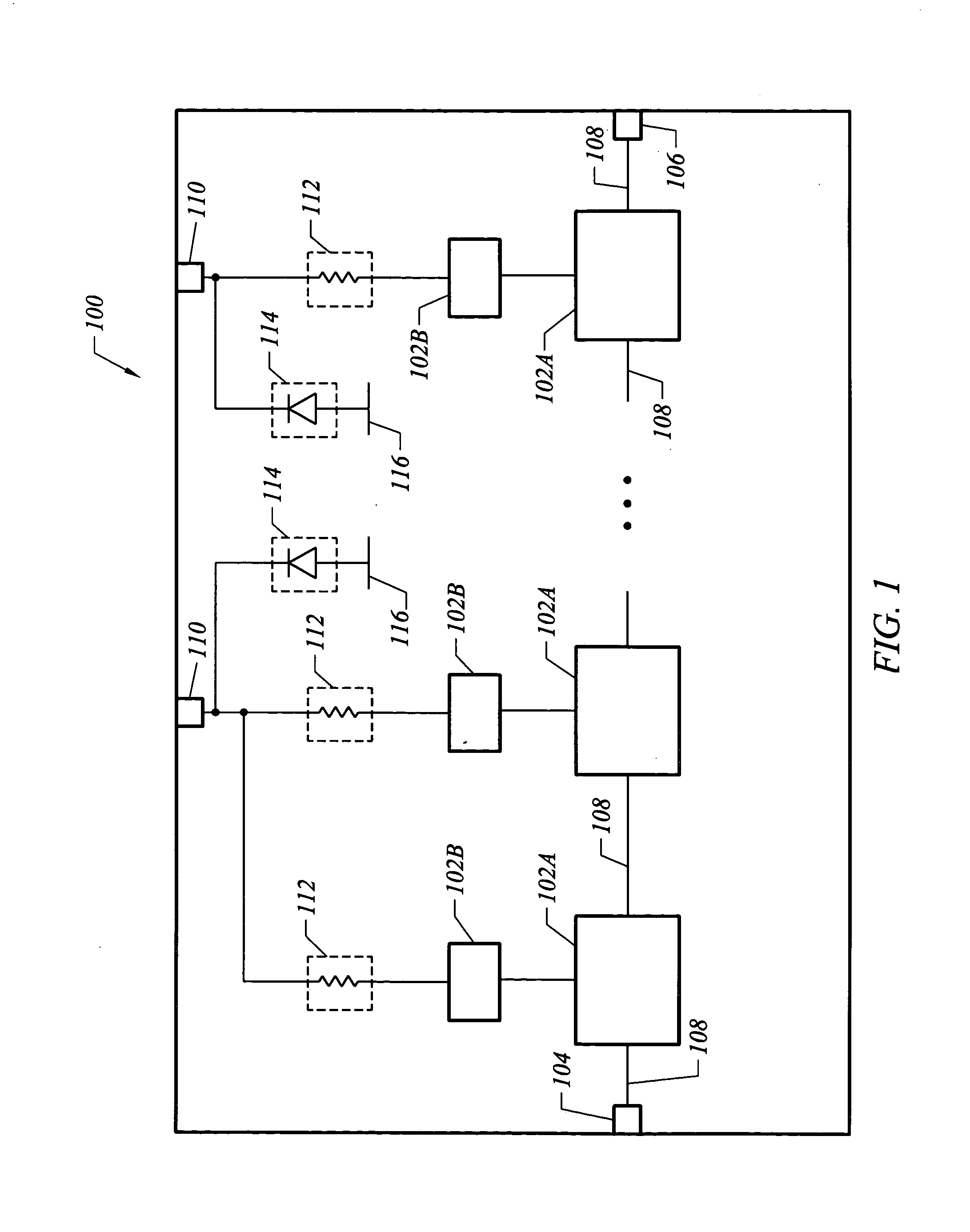
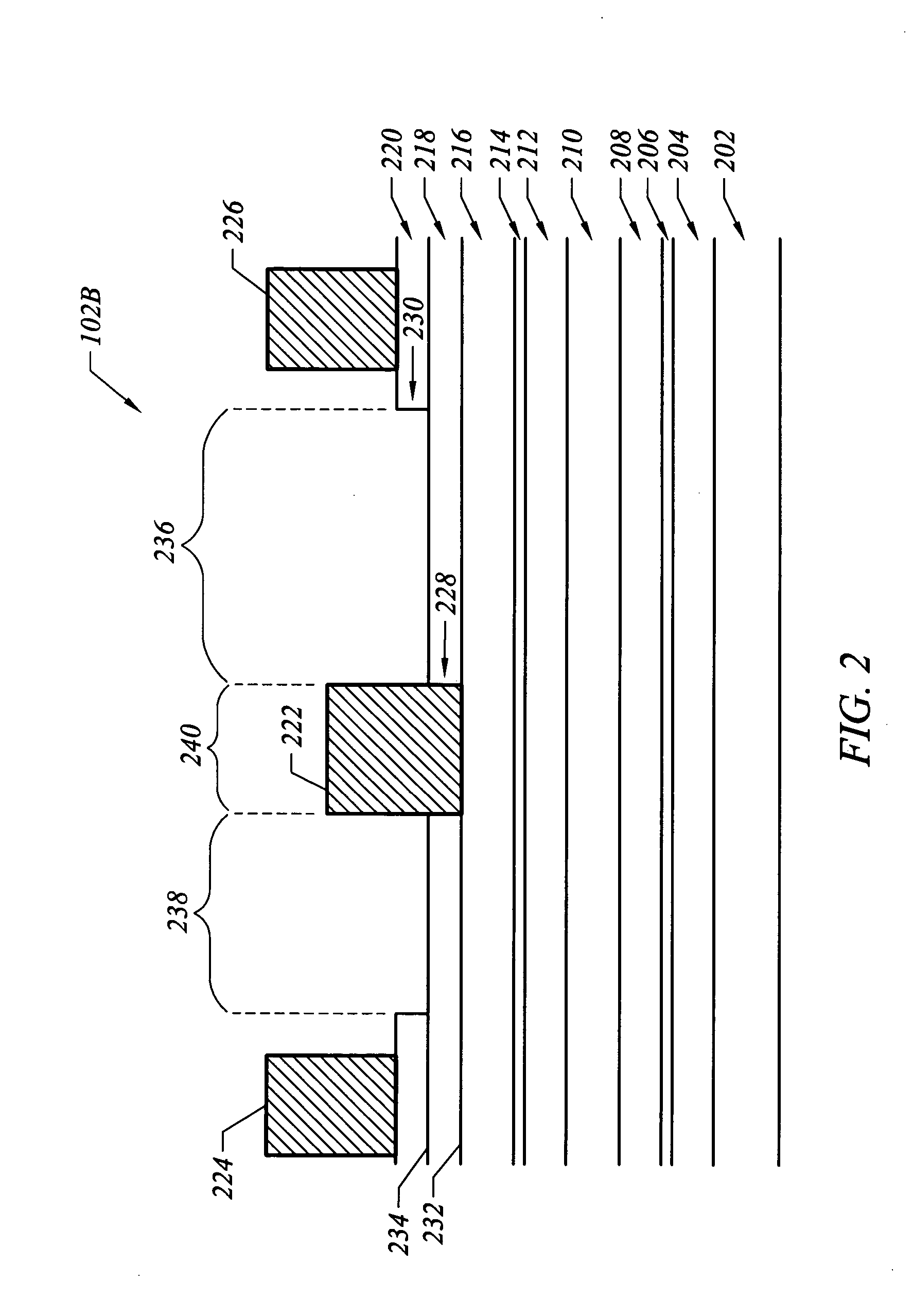
[0013] With reference to FIG. 1, an integrated circuit (IC) 100 with enhancement mode pseudomorphic high-electron mobility transistors (E-pHEMTs) 102A and 102B in accordance with an embodiment of the invention is described. As an example, the IC 100 may be a radio frequency (RF) IC such as a power amplifier RFIC for amplification of RF signals. However, the IC 100 may be any type of IC with any functionality or functionalities. As described in more detail below, the IC 100 has on-chip electrostatic discharge (ESD) protection that minimizes the use of chip area for the ESD protection.

[0014] The IC 100 includes an input node 104 that receives input signals, such as input RF signals, and an output node 106 that transmits output signals, such as amplified RF signals. The IC further 100 includes a number of active components in the form of E-pHEMTs 102A and 102B. Some of these E-pHEMTs are located on a signal path 108 from the input node 104 to the output node 106. These E-pHEMTs 102A a...


PUM


Abstract

An integrated circuit (IC) with high electron mobility transistors, such as enhancement mode pseudomorphic high electron mobility transistors (E-pHEMTs) and method for fabricating the IC utilizes an increased gate-to-drain etch recess spacing in some of the high electron mobility transistors to provide on-chip electrostatic discharge protection. The use of the increased gate-to-drain etch recess spacing allows smaller high electron mobility transistors to be used for ancillary low speed applications on the IC, which reduces the chip area occupied by these ancillary transistors.

Description

BACKGROUND OF THE INVENTION [0001] Enhancement mode pseudomorphic high electron mobility transistors (E-pHEMTs) provide operating properties suited for portable wireless applications, such as radio frequency applications. E-pHEMTs require less power to operate than other comparable devices, and consequently, can be used to produce power amplifiers with an exceptional power-added efficiency, which is a measure of how much power is needed to achieve a given amount of amplification. Furthermore, in contrast to other similar devices, E-pHEMTs can operate from a single positive voltage supply since the E-pHEMTs do not require negative gate voltage for control. Thus, E-pHEMTs can be operated without components that provide a negate voltage supply, which translates into decrease in system cost, reduced board space requirements and less complex system design. Due to these operating properties, E-pHEMTs are currently used in radio frequency integrated circuits (RFICs) for portable wireless d...

Claims


Application Information

Patent Timeline
Patent Type & Authority Applications(United States)
IPC IPC(8): H01L21/335H01L27/04H01L21/338H01L21/822H01L27/02H01L27/095H01L29/08H01L29/778H01L29/812H01L31/0328
CPCH01L27/0248H01L29/7785H01L29/66462
Inventor PARK, CHUL HONG
Owner AVAGO TECH WIRELESS IP SINGAPORE PTE
Features
  • Generate Ideas
  • Intellectual Property
  • Life Sciences
  • Materials
  • Tech Scout
  • Unparalleled Data Quality
  • Higher Quality Content
  • 60% Fewer Hallucinations
Learn More