Contact-bonded optically pumped semiconductor laser structure
- Summary
- Abstract
- Description
- Claims
- Application Information
AI Technical Summary
Benefits of technology
Problems solved by technology
Method used
Image

Examples
Embodiment Construction
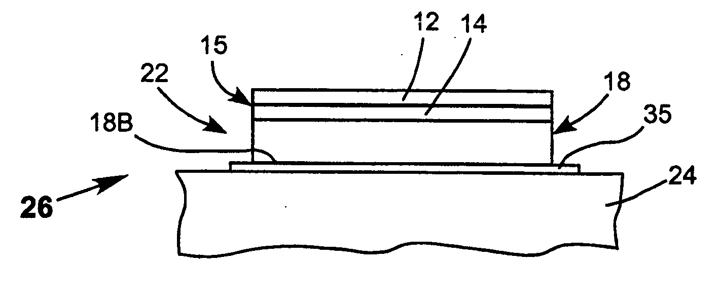
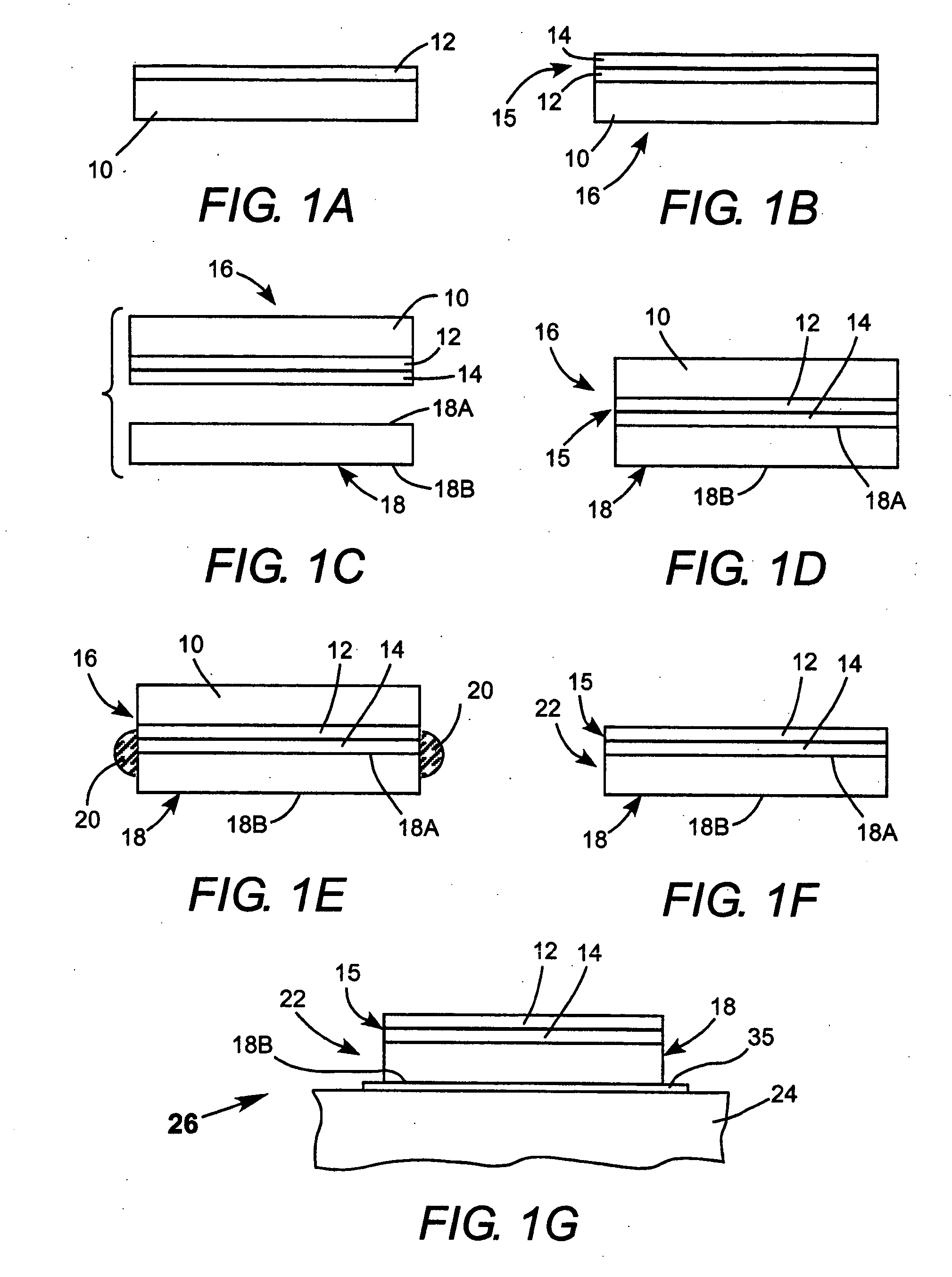
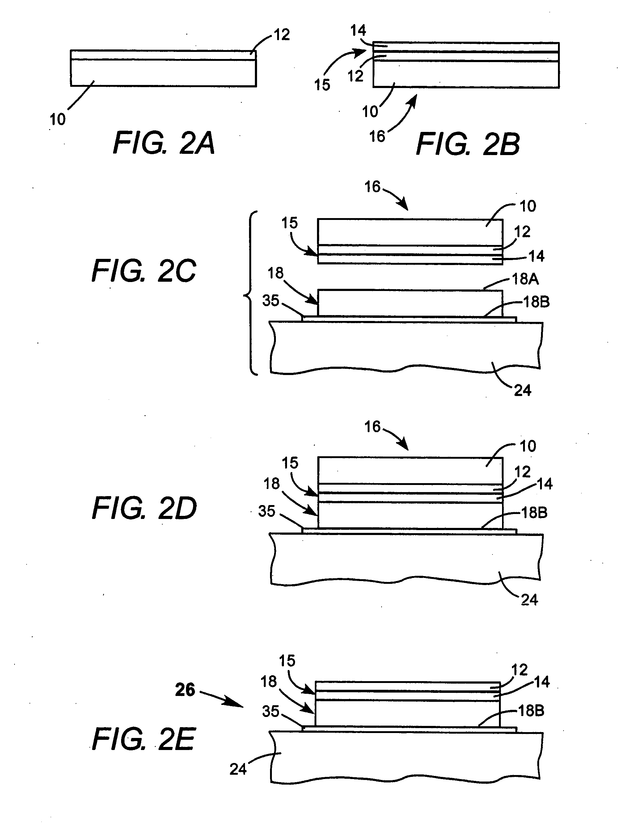
[0014] Referring now to the drawings, wherein like features are designated by like reference numerals, FIGS. 1A-G schematically illustrate one preferred method in accordance with the present invention of fabricating an assembly 26 of an OPS-structure 15 on a heat sink 24 (see FIG. 1G). OPS-structure 15 includes a gain-structure 12 and a Bragg mirror structure 14. A diamond heat spreader 18 is located between Bragg mirror structure 14 of OPS-structure 15 and the heat sink. Heat spreader 18 preferably has a thickness greater than about 300 micrometers (Jim). Fabrication steps are as follows.
[0015] Multilayer gain-structure 12 is epitaxially grown on a single crystal substrate 10 (see FIG. 1A). The material of the substrate is selected according to the material of the layers the OPS-structure. The substrate material, for example, may be gallium arsenide (GaAs) or Indium Phosphide (InP). Next, Bragg mirror structure 14 is deposited or grown on gain-structure 12 see (FIG. 1B) forming an...
PUM
 Abstract
Description
Claims
Application Information