

Backside rapid thermal processing of patterned wafers
a technology of patterned wafers and backsides, applied in the field of heat treatment of semiconductor wafers, can solve the problems of increasing difficult fabrication constraints, requiring further and tighter control, and varying emissivity or absorption on the front side of the wafer, and achieving the effect of reducing the number of patterned wafers
- Summary
- Abstract
- Description
- Claims
- Application Information
AI Technical Summary
Benefits of technology
Problems solved by technology
Method used
Image

Examples
Embodiment Construction
[0024] The uniformity of rapid thermal processing (RTP) is greatly enhanced if the unpatterned back side of the wafer is positioned to face the radiant heat source and the patterned front side faces a reflector and is dynamically monitored for its temperature.
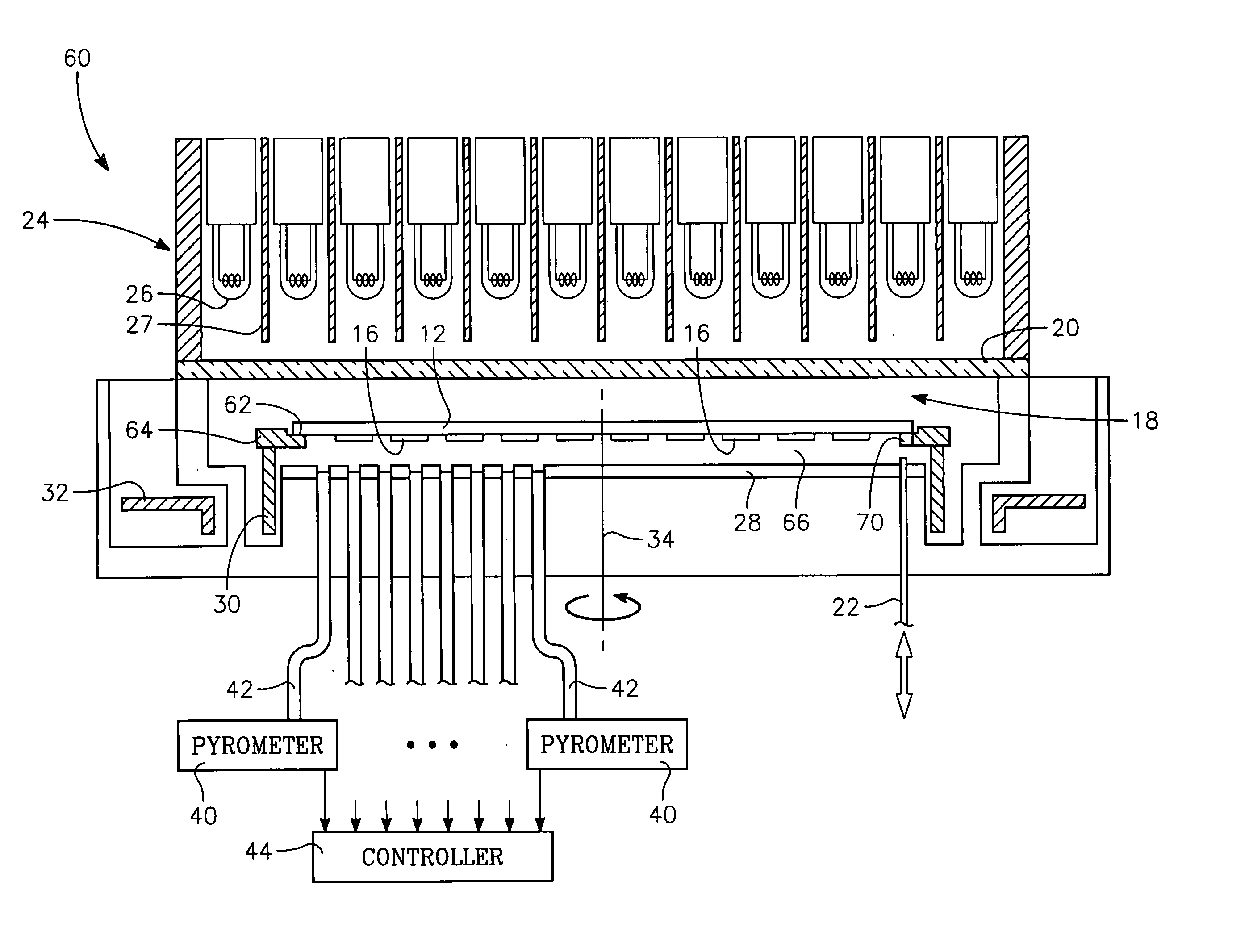
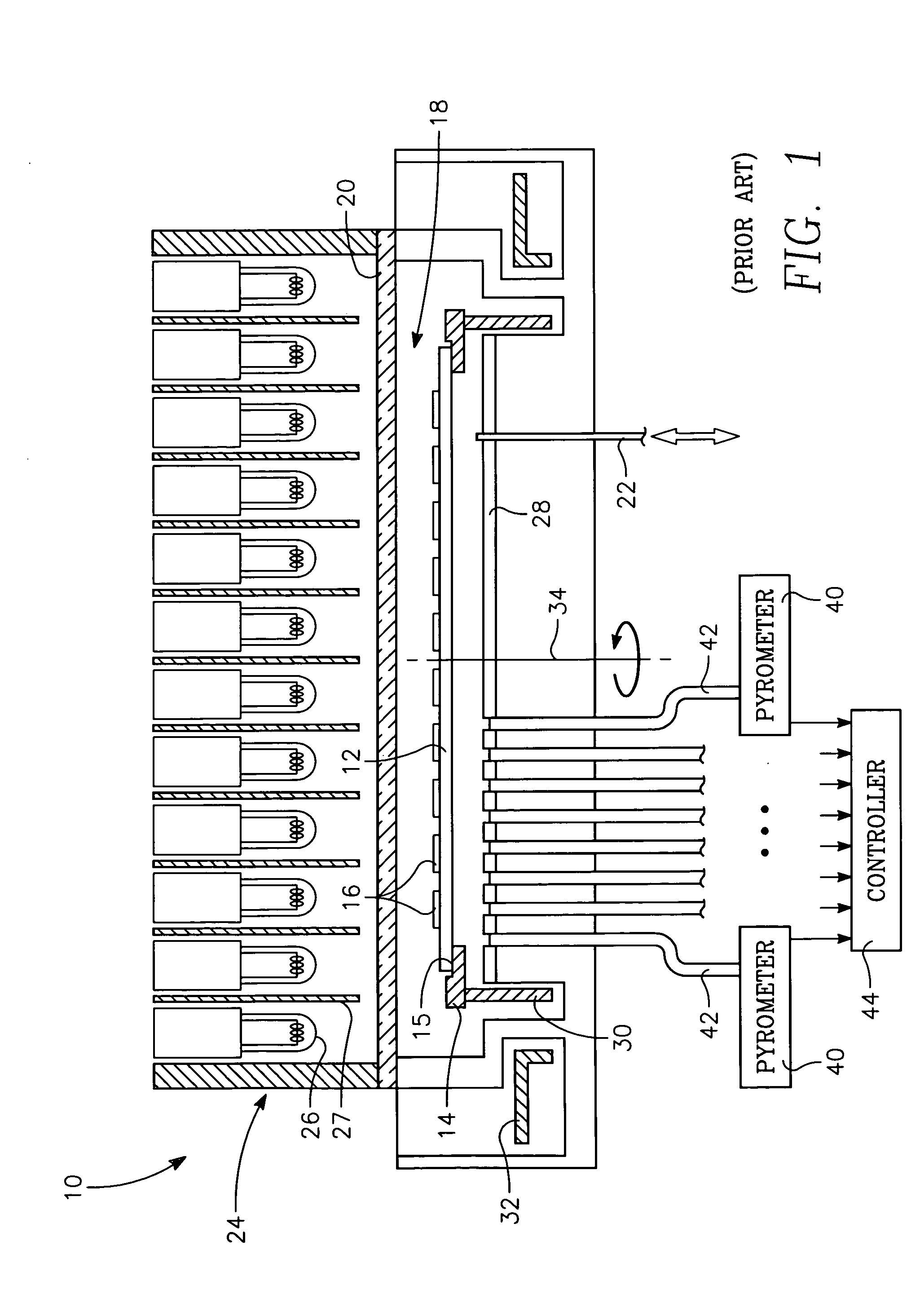
[0025] As illustrated in the schematic cross-sectional view of FIG. 3, backside RTP can be effected within an RTP reactor 60 that differs in only a few ways from the reactor 10 of FIG. 1 for front side processing.
[0026] In one embodiment, a generally annular and sloping shelf 62 of an edge ring 64, as better illustrated in the cross-sectional view of FIG. 4, supports a beveled corner of the inverted wafer 12 oriented with its features 16 constituting the developing integrated circuits facing downwardly toward the reflector plate 28. The edge ring shelf 62 is generally shortened over the conventional shelf 15 so that edge ring shelf 62 shields the wafer 12 from the reflector 28 by a distance V that less than the wafer edge exc...
PUM
 Abstract
Description
Claims
Application Information