Periodic interleaved star with vias electromagnetic bandgap structure for microstrip and flip chip on board applications

a technology of interleaved stars and flip chips, applied in cross-talk/noise/interference reduction, waveguide devices, printed circuit aspects, etc., can solve problems such as unique electromagnetic resonance and emission packaging problems, potential formation of electromagnetic boundaries, and degradation of semiconductor performan

Active Publication Date: 2005-09-08
RAYTHEON CO
View PDF5 Cites 61 Cited by
  • Summary
  • Abstract
  • Description
  • Claims
  • Application Information

AI Technical Summary

Benefits of technology

[0015] Above limitations are improved by a hybrid assembly comprising a single electromagnetic band gap (EBG) layer on a substrate having an upper surface and a lower surface and a semiconductor structure (MMIC) mount

Problems solved by technology

While bumps are advantageous as compared to wire inter-connections, their presence between a semiconductor structure and a host substrate presents unique electromagnetic resonance and emission packaging problems.
A particular difficulty introduced by the semiconductor structure mounted on the host substrate is the potential formation of electromagnetic boundaries which support unwanted, parallel plate, waveguide like (surface modes) of energy propagation.
Such unwanted modes can propagate near the surface of the host substrate causing degradation in semiconductor performance because of signal interference.
The degradation in semiconductor performance are caused by unwanted signal transfer among semiconductor structure inputs and outputs, affecting gain and phase response, loss of isolation between adjacent paths in multiple path / multiple channel circuit applications, and circuit instability.
These negative effects are due to the introduction of unwanted coupling or feedback paths.
Maximum frequency operation of the semiconductor in the presence of these unwanted feedback paths are undesirably dependent on the dimensions of the semiconductor structure.
Thus, semiconductor structures with large dimensions with respect to wavelength operating frequency present a potential difficulty.
This difficulty is prevalent with fast Gallium Arsenide (GaAs) semiconductor structures mounted on a host substrate.
Near cutoff, the semiconductor structure may be functional, but unable to operate because the incoming signals are interfering with each other.
Unfortunately, because of semiconductor structure limitations and assembly requirements, this practice of using redundant ground bumps as obstacles to surface propagated electromagnetic waves results in a further increase in both semiconductor structure and substrate size, increasing weight, power consumption and reducing reliability of the resulting hybrid.
The limitation here is that a plurality of of EBG layers may have to be used to achieve the level of attenuation desired.

Method used


Image

  • Periodic interleaved star with vias electromagnetic bandgap structure for microstrip and flip chip on board applications
  • Periodic interleaved star with vias electromagnetic bandgap structure for microstrip and flip chip on board applications
  • Periodic interleaved star with vias electromagnetic bandgap structure for microstrip and flip chip on board applications

Examples


Embodiment Construction

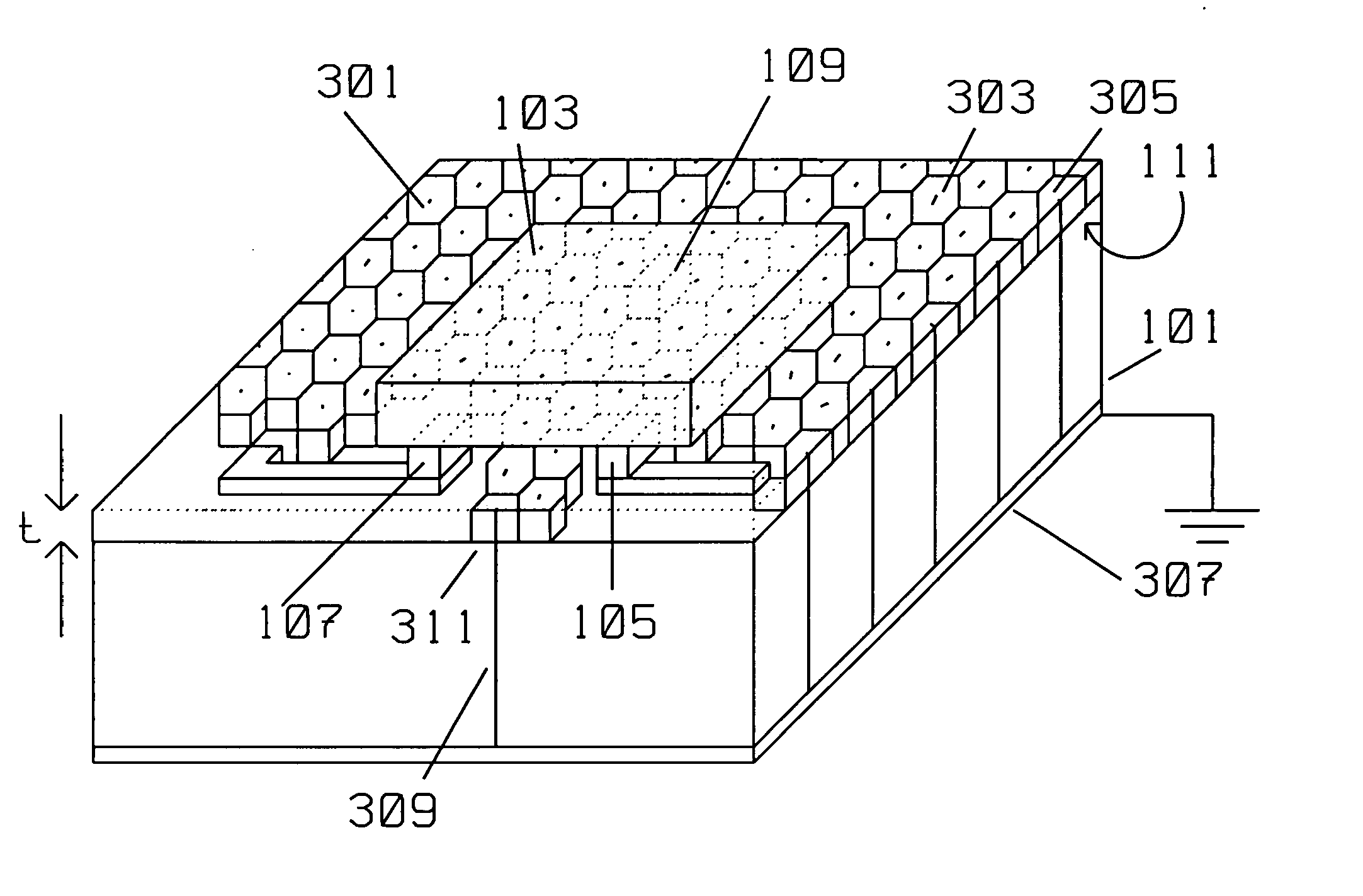
[0025] The present invention describes an apparatus and method for improved cross talk suppression in a hybrid assembly by incorporating a single layer made of electromagnetic band-gap (EBG) stars on a hybrid substrate such as, for example, alumina, LTCC (low temperature co-fired ceramic) as well as HTCC (high temperature co-fired ceramic).

[0026] The EBG stars reduce the cross talk induced by undesired surface / waveguide modes at high operating frequencies (10 to 20 Ghz) between input / output and power (or ground) pins on the operation of the hybrid.

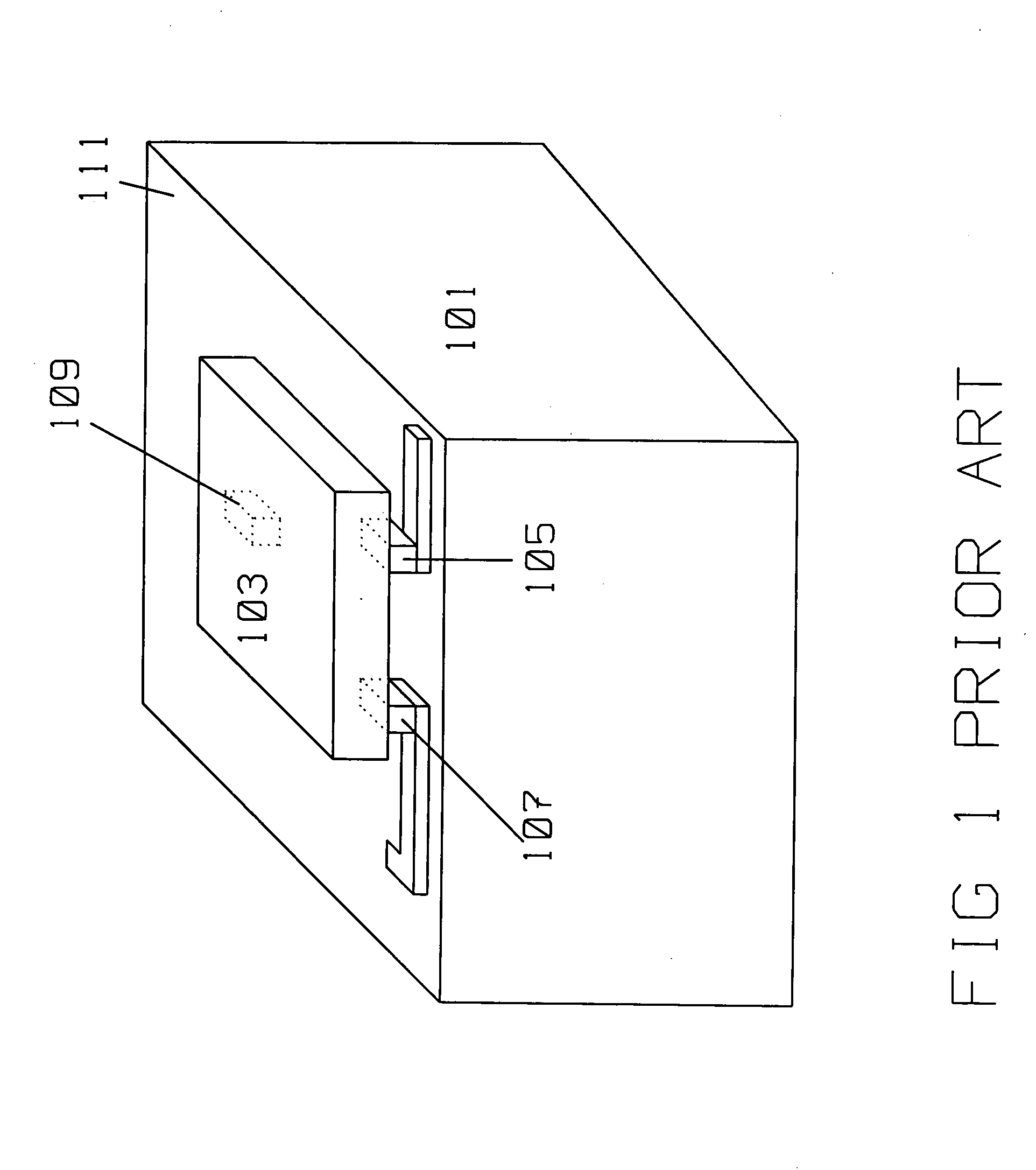
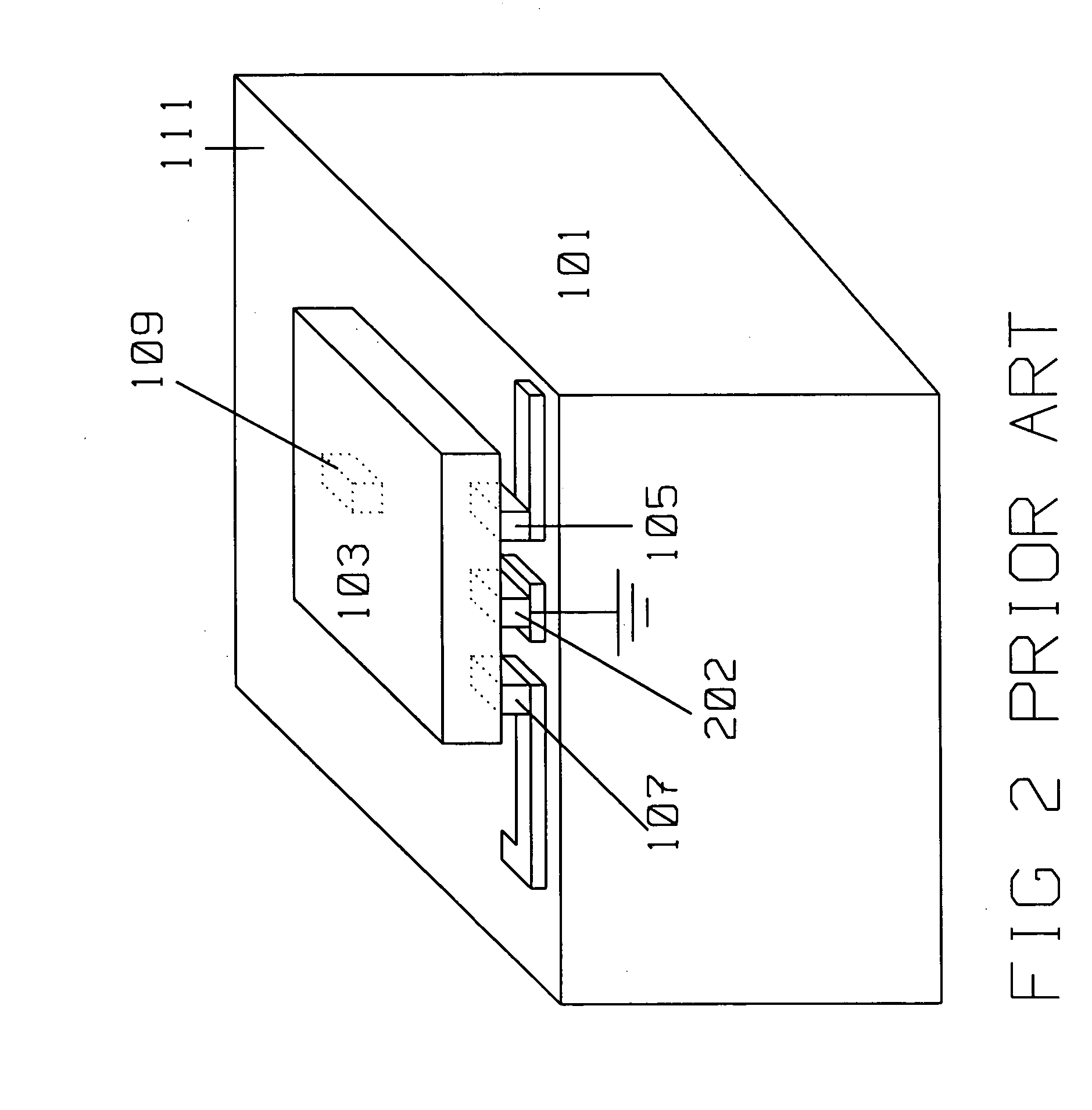
[0027]FIG. 1 is a typical configuration of a hybrid of the prior art where a semiconductor structure 103 is mounted on the upper surface 111 of a host substrate 101 using bumps 105, 107 and 109 for inter-connection means. Substrate 101 has an upper metalization layer deposited on upper surface 111 of substrate 101. Conductive paths 113 and 115 are etched from a metalization layer, and interconnect bumps 105, 107 and 109 to their respecti...


PUM


Abstract

A hybrid assembly having improved cross talk characteristics includes an electromagnetic band gap (EBG) layer on a substrate having an upper surface and a lower surface and a semiconductor structure (MMIC) mounted above the EBG layer. A plurality of stars made of an EBG material are preferably printed, or deposited, on the upper surface. The EBG material has slow wave characteristics. The plurality of stars tessellates the upper surface between conductive paths. Each of the stars has a center section formed from a regular polygon, the center section having projections extending from the center section. The projections and the center section form a periphery. The periphery engages adjacent stars along the periphery. Stars are separated from adjacent stars by an interspace. Each of the stars is connected to a conductive via, in turn connected to ground potential. A conductive layer at ground potential is electrically continuous with vias used to interconnect all stars forming the EBG layer.

Description

[0001] This application is a continuation in part of parent application titled “Improved Flip Chip MMIC on Board Performance Using Periodic Electromagnetic Bandgap Structures” filed ______ 2004, Ser. No. ______.BACKGROUND OF THE INVENTION [0002] 1. Field of Invention [0003] This invention is in the field of cross-talk suppression in a hybrid assembly at microwave frequencies. [0004] 2. Description of the Related Art [0005] Monolithic Integrated Circuits (MMIC), an example of a semiconductor structure, support many of the present generation of military and commercial radio frequency sensors and communication applications. MMICs include active devices, such as field effect transistors and bipolar transistors, passive elements such as capacitors, thin film / bulk resistors, and inductors integrated on a single semi-insulating substrate, such as Gallium Arsenide. [0006] Hybrid technology relates to methods used for interconnecting a plurality of separate semiconductor structures, such as ...

Claims


Application Information

Patent Timeline
IPC IPC(8): H01L23/00H01L23/14H01L23/498H01L23/50H01L23/552H01L23/66H05K1/02H05K1/03H05K1/09H05K9/00
CPCH01L23/49838H01L23/50H01L2924/1305H01L23/552H01L23/66H01L2224/16237H01L2224/81801H01L2924/01079H01L2924/09701H01L2924/3025H01P1/2005H05K1/0236H05K1/0306H05K1/09H05K2201/0715H05K2201/09336H05K2201/09681H01L2224/16225H01L2924/00H01P1/16
Inventor TONOMURA, SAMUEL D.
Owner RAYTHEON CO
Why Eureka
Try Eureka