Method for fabricating embedded thin film resistors of printed circuit board
a printed circuit board and embedded technology, applied in the field of printed circuit boards, can solve the problems of difficult to achieve constant and precise resistances of resistors, high price, and easy high temperature exposure of printed circuit board lamination, and achieve the effect of reducing the size of the circuit, reducing the risk of failure, and improving the quality of the printed circuit board
- Summary
- Abstract
- Description
- Claims
- Application Information
AI Technical Summary
Benefits of technology
Problems solved by technology
Method used
Image
Examples
first embodiment
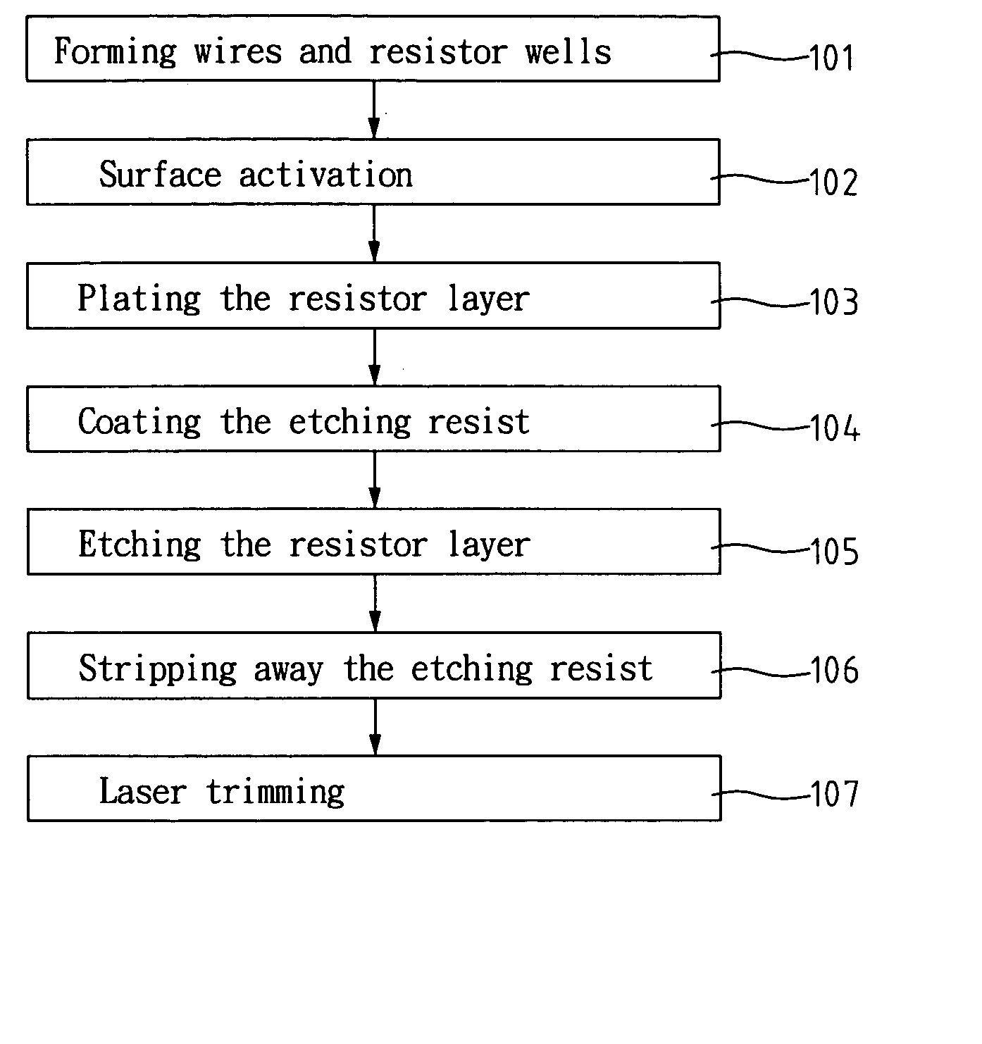
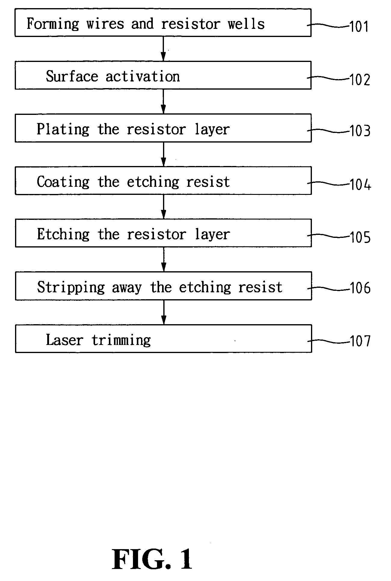
[0013]FIG. 1 is a flow chart showing the steps of forming embedded thin film resistors on a printed circuit board according to the present invention. These steps are described sequentially as follows.
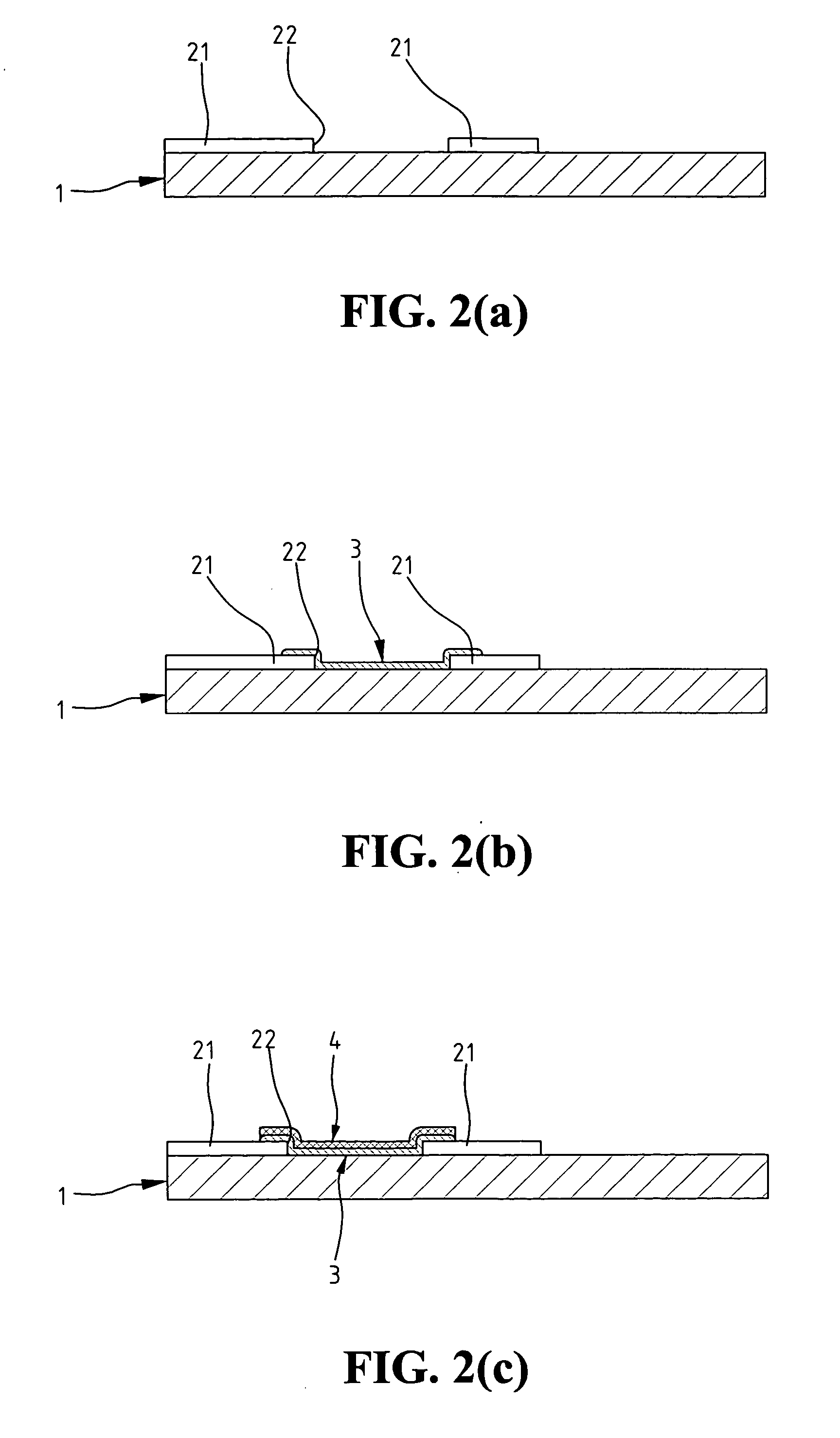
[0014] In step 101, as shown in FIG. 2(a), the conductive wires 21 with resistor wells 22 are formed on a substrate made of an insulating polymer according to layout requirement of circuitry.
[0015] The foregoing conductive wires 21 and resistor wells 22 can be formed using an ordinary printed circuit board fabrication process such as the subtractive, additive, or semi-additive process. The conductive wire 21 is made of copper, aluminum, other well conductive material, or an alloy of the above.
[0016] In step 102, as shown in FIG. 2(b), an activated layer 3 is coated on top of at least surface of each resistor well 22 so as to activate the insulating polymer of the substrate 1 exposed by each resistor well 22.
[0017] The foregoing activated layer 3 is made of activated palladium (Pd) or...
second embodiment
[0027]FIG. 3 is a flow chart showing the steps of forming embedded thin film resistors on a printed circuit board according to the present invention. These steps are described sequentially as follows.
[0028] In step 201, as shown in FIG. 4(a), a conductive layer 2 is formed on a substrate 1 made of an insulating polymer. The conductive layer 2 is then processed, based on the locations and dimensions of the resistors required by the printed circuit board, to form the corresponding resistor windows 23.
[0029] The conductive layer 2 is made of copper, aluminum, other well conductive material, or an alloy of the above.
[0030] In step 202, as shown in FIG. 4(b), an activated layer 3 is coated on top of at least surface of each resistor window 23 of the conductive layer 2 so as to activate the insulating polymer of the substrate 1 exposed by each resistor window 23.
[0031] The foregoing activated layer 3 is made of activated palladium (Pd) or other appropriate activator that can be used to...
PUM
| Property | Measurement | Unit |
|---|---|---|
| Thickness | aaaaa | aaaaa |
| Electrical resistance | aaaaa | aaaaa |
| Shape | aaaaa | aaaaa |
Abstract
Description
Claims
Application Information


