Circuit board and method for manufacturing the same

a technology of circuit boards and manufacturing methods, applied in the field of circuit boards, can solve the problems of increasing the minuteness of printed boards (circuit boards), increasing the cost of materials, and increasing the cost of manufacturing costs including installation costs and material costs

Inactive Publication Date: 2005-09-15
PANASONIC CORP
View PDF2 Cites 12 Cited by
  • Summary
  • Abstract
  • Description
  • Claims
  • Application Information

AI Technical Summary

Benefits of technology

[0022] In order to solve the above-described conventional problems, the present invention provides a circuit board in which very small vias and conductors can be formed and a method for manufacturing such a circuit board.

Problems solved by technology

In particular, the increasing minuteness of printed boards (circuit boards) is advancing due to the rapid increase in the number of leads drawn from these semiconductor devices and the number of terminals.
However, these technologies have the following problems.
With this technique, although it is indeed possible to form a wiring pattern with a laser, in addition to a high energy output laser (a highest output of 100 W with a Nd: YAG laser) being necessary, the material costs become higher than the costs of materials normally used for printed boards, and therefore manufacturing costs including installation costs and material costs become higher, and it would be extremely difficult to manufacture a product that could replace the printed boards being used today.
Further still, there also is the problem that the wiring here has a comparatively large resistance value.
However, compared to the printed boards that are widespread today, diamond coat printed circuit boards require a special manufacturing process to form the diamond thin film, which presents considerable problems in terms of manufacturing costs.
Furthermore, since irradiation is carried out with an argon laser when carrying out laser irradiation, compared to laser irradiation with semiconductor lasers that have considerably smaller output than argon lasers, the laser irradiation process is a comparatively large-scale process.
In addition to this, the resistance value of the (graphite) portions of formed wiring patterns that have changed to blackish due to laser irradiation is approximately 3 ohm / cm, so there is also the problem of a comparatively large resistance value.
However, with this technique, obtaining electrical conductivity that can be used for wiring is difficult or complicated.
However, it is difficult to obtain an electrical conductivity that can be used as wiring for a printed board with a material made of such a conductive polymer.
On the other hand, in interlayer connection technologies that use vias, there are not only merely cost-related issues in forming miniaturized vias above the current level, but also technological difficulties.
This is because there is a limit to the miniaturization of via formation related to physical hole processing since either a technique is used in which vias are formed by plating after a drilling process or a technique is used in which vias are formed by plating after laser processing.
Although there are also techniques in which excimer lasers or the like are used, these are unlikely to be used in practice due to considerations of high cost.
Furthermore, if the holes (via holes) are to be made small, there is the problem that the smaller the holes become, the more difficult it is to fill the holes with a conductive material.
When filling the holes with a conductive material using plating, considering the permeation conditions of the plating liquid, it is difficult to fill the holes well unless the aspect ratio is 2 or lower.
Even when filling the holes with a conductive material using a conductive paste, holes with a diameter of at best 50 μm can be filled, and it is extremely difficult technologically to fill holes of 30 μm or smaller with the conductive material.
If reducing the surface area of circuit boards is desired as part of miniaturizing electronic devices, the limit dimension of via diameters becomes a bottleneck to design when the diameter of vias cannot be made more minute than current levels.
In other words, being unable to form extremely minute vias easily has become an obstacle to miniaturizing circuit boards.

Method used


Image

  • Circuit board and method for manufacturing the same
  • Circuit board and method for manufacturing the same
  • Circuit board and method for manufacturing the same

Examples


Embodiment Construction

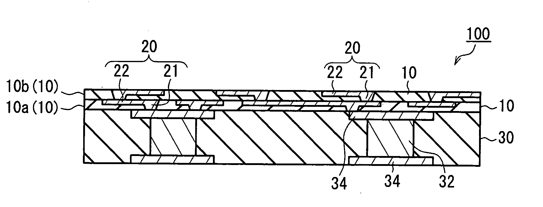
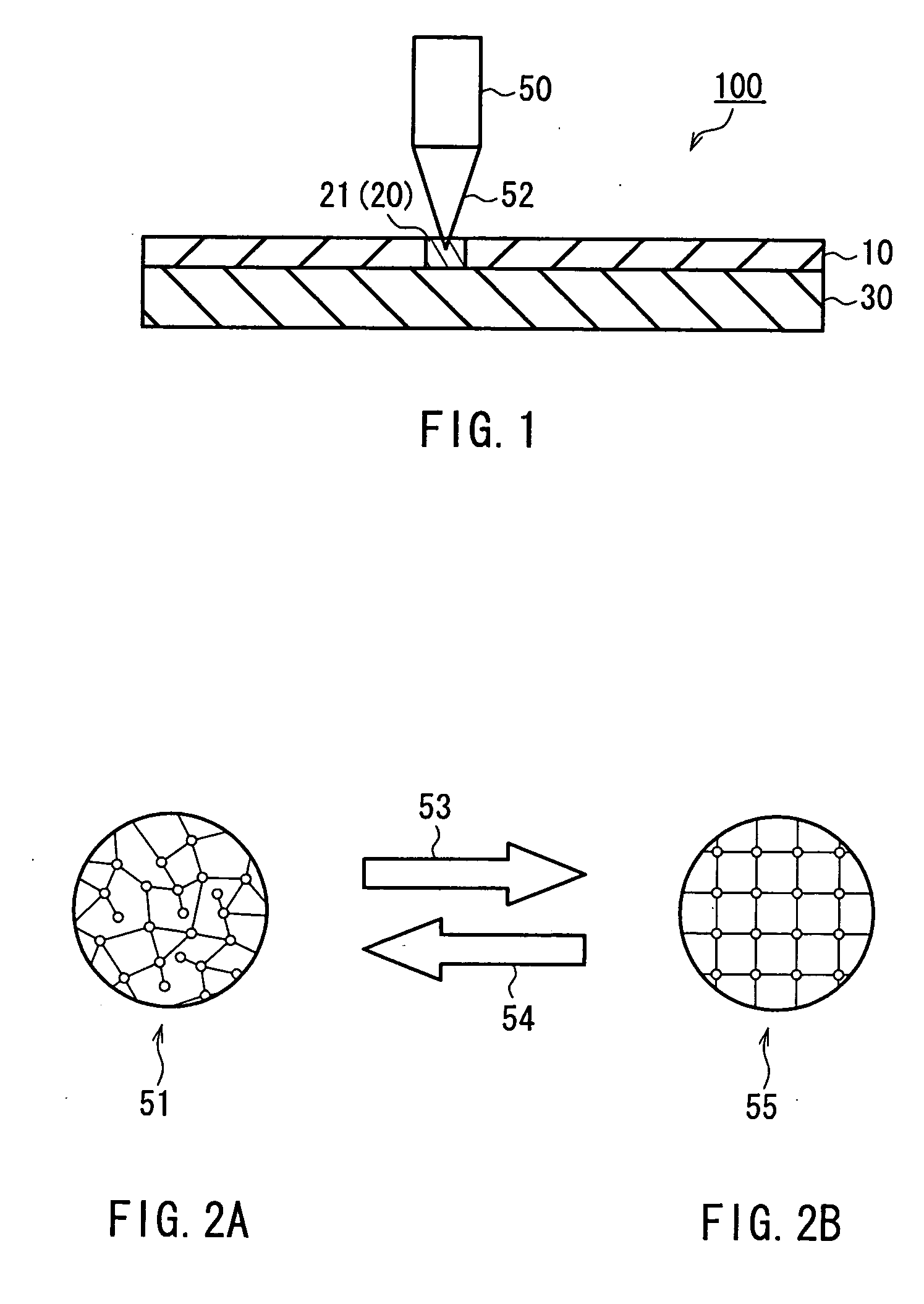
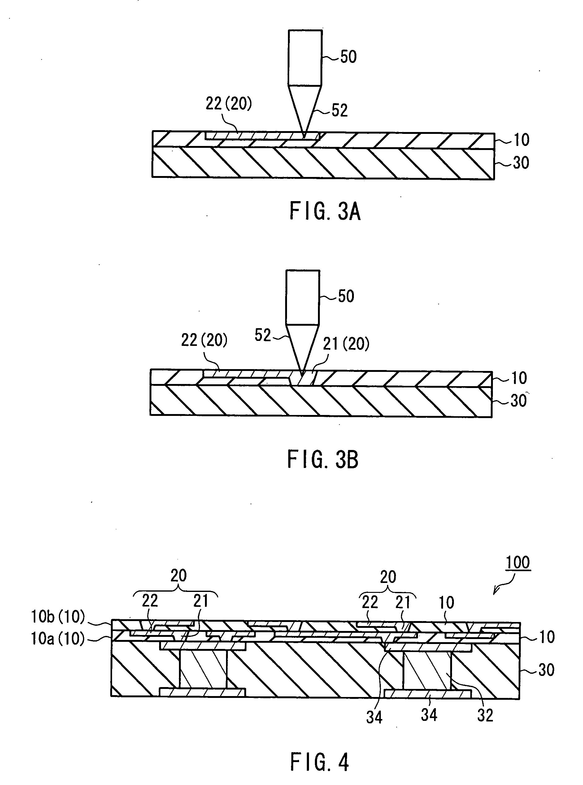
[0056] With the present invention, a conductive path is formed by irradiating laser light onto a phase change layer using phase change in a phase change layer formed from a phase change material that is capable of changing alternately between an electrically insulating state and an electrically conductive state, and therefore very small-dimension minute vias and conductors can be formed. Furthermore, the phase change of a chalcogenide semiconductor according to the present invention is reversible, and therefore subsequent repair, rework, or trimming also is easy. As a result, production yields can be improved.

[0057] A circuit board according to the present invention can be used singly by itself and also can be used formed on a substrate. When used singly by itself, it is first constructed on a temporary substrate then transferred to a final substrate.

[0058] In a preferred embodiment of the present invention, the conductive path is at least one of a via and a conductor, and the pha...


PUM

PropertyMeasurementUnit
electrical conductivityaaaaaaaaaa
resistanceaaaaaaaaaa

Abstract

In a circuit board according to the present invention, on a substrate, in at least a portion of a phase change layer including a phase change material that is capable of changing alternately between an electrically insulating state and an electrically conductive state, a conductive path is formed that has been put into an electrically conductive state by a phase change in the phase change layer, wherein the phase change material includes a chalcogenide semiconductor, changes between the electrically insulating state and the electrically conductive state by irradiation of laser light, goes into the electrically conductive state in a crystalline phase, and goes into the electrically insulating state in an amorphous phase. In this way, a conductive path is formed by irradiating laser light onto a phase change layer using phase change in a phase change layer formed from a phase change material that is capable of changing alternately between an electrically insulating state and an electrically conductive state, and therefore very small-dimension minute vias and conductors can be formed. Furthermore, subsequent repair, rework, or trimming also is easy.

Description

BACKGROUND OF THE INVENTION [0001] 1. Field of the Invention [0002] The present invention relates to circuit boards for the mounting of electronic components such as semiconductor devices for example, and to methods for manufacturing such circuit boards. [0003] 2. Description of the Related Art [0004] Along with the miniaturization and increasingly high functionality of electronic equipment in recent years, there have been advances in increasing the number of pins in the semiconductor devices that constitute such electronic equipment and in miniaturization of such components, and the number and density of the wires of the printed boards on which these are mounted are increasing dramatically. In particular, the increasing minuteness of printed boards (circuit boards) is advancing due to the rapid increase in the number of leads drawn from these semiconductor devices and the number of terminals. [0005] Today's most leading edge fine pitch level is a pitch in the range of 40 to 50 μm i...

Claims


Application Information

Patent Timeline
Patent Type & Authority Applications(United States)
IPC IPC(8): H01L21/48H01L23/14H05K1/00H05K1/09H05K1/16H05K3/00H05K3/10H05K3/40H05K3/46
CPCH05K1/167H05K3/105H05K3/4038H05K3/4644Y10T29/49126H05K2203/107H05K2203/171Y10T29/49155Y10T29/49165H05K2201/0326
Inventor ISHIMARU, YUKIHIRONAKATANI, SEIICHISAITO, YOSHIYUKI
Owner PANASONIC CORP
Why Eureka
Try Eureka