Semiconductor laser element having InGaAs compressive-strained quantum-well active layer

Inactive Publication Date: 2005-09-15
FUJIFILM HLDG CORP +1
View PDF3 Cites 13 Cited by
  • Summary
  • Abstract
  • Description
  • Claims
  • Application Information

AI Technical Summary

Benefits of technology

[0015] In the semiconductor laser elements according to the first and second aspects of the present invention, the active layer is made of InGaAs, which realizes the oscillation wavelength of 0.9 to 1.2 micrometers. In addition, the active layer has a compressive-strain quantum-well structure. Therefore, the efficiency in carrier confinement is enhanced, and the threshold current can be maintained low. Further, since the current-blocking layer arranged on both sides of the active layer reduces leakage current, heat generation in the semiconductor laser elements is suppressed, and satisfactory temperature characteristics are obtained. Thus, satisfactory optical-output characteristics are stably obtained even in a high temperature environment, and power consumption can be suppressed.
[0016] In addition, it is preferable to arrange a carrier-confinement layer (which may be referred to as a carrier-blocking layer) between the active layer and each of the lower and upper optical waveguide layers. The efficiency in carrier confinement is remarkably increased by the provision of the carrier-confinement layer. At this time, when the current-blocking layer is made of AlGaInP, the effect of suppressing the leakage current is further enhanced, and therefore the characteristics of the semiconductor laser element are further improved.
[0017] Specifically, it is preferable to form each carrier-confinement layer of a material which has a bandgap greater than the bandgap of each of the lower optical waveguide layer and the upper optical waveguide layer, and smaller than the bandgap of each of the lower claddi

Problems solved by technology

However, even when the processing speeds of the CPUs per se are increased, the substantial processing speeds of computers do not increase unless the data transfer rates between each CPU and other elements, such as memories and LSIs (large-scale integrated circuits) for image processing, increase.
Therefore, there is concern about the influence of the heat generated by the LSIs.
However, the surface-emitting semiconductor lasers have structural constraints which increase resistance.
The

Method used


Image

  • Semiconductor laser element having InGaAs compressive-strained quantum-well active layer
  • Semiconductor laser element having InGaAs compressive-strained quantum-well active layer
  • Semiconductor laser element having InGaAs compressive-strained quantum-well active layer

Examples


first embodiment

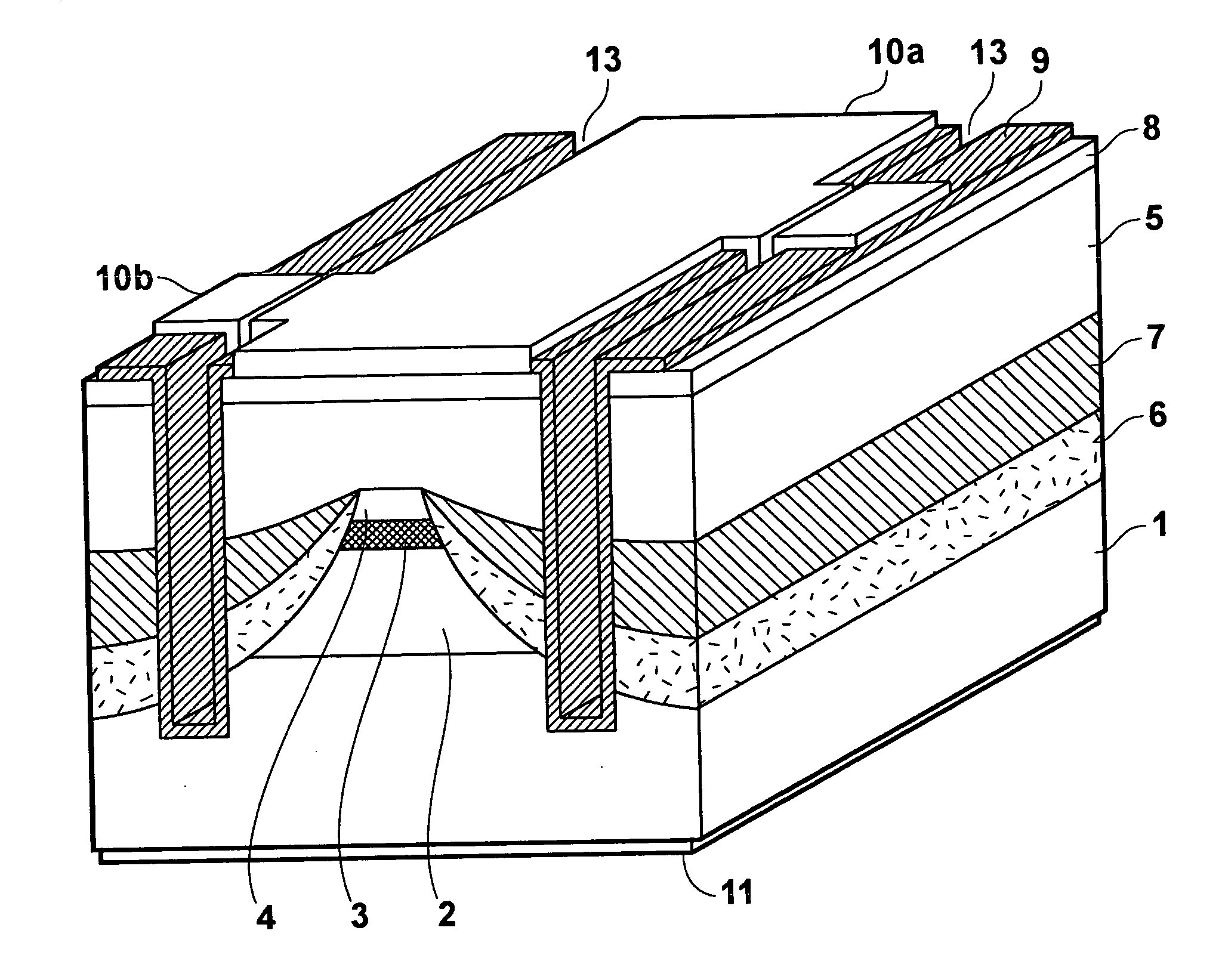
[0029]FIG. 1 is a schematic perspective view of the semiconductor laser element according to the first embodiment of the present invention.

[0030] As illustrated in FIG. 1, the semiconductor laser element according to the present embodiment contains a stripe-shaped, layered structure in which an n-type In0.49Ga0.51P lower cladding layer 2 having a thickness of 2.0 micrometers and being doped with impurity of 1×1018 cm−3, a light-emission layer 3 having a thickness of about 100 nm, a p-type In0.49Ga0.51P first upper cladding layer 4 having a thickness of 1.0 micrometers and being doped with impurity of 1×1018 cm−3, and a p-type GaAs cap layer (not shown) having a thickness of 10 nm and being doped with impurity of 1×1018 cm−3 are formed in this order on an n-type GaAs substrate 1. As illustrated in FIG. 1, the stripe widths of the n-type In0.49Ga0.51P lower cladding layer 2, the light-emission layer 3, the p-type In0.49Ga0.51P first upper cladding layer 4, and the p-type GaAs cap lay...

second embodiment

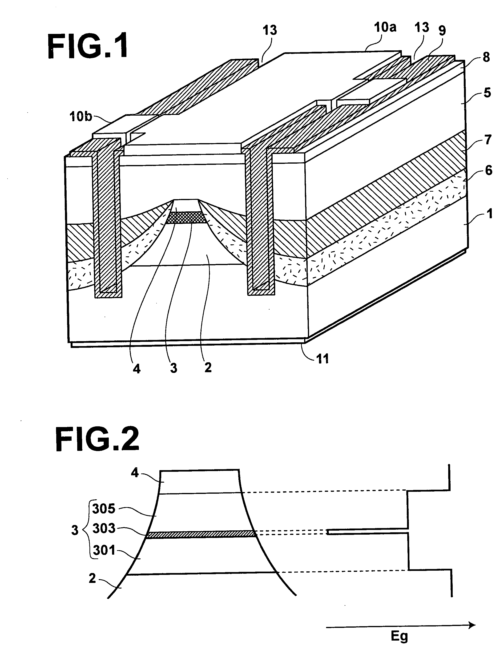
[0041] Next, the semiconductor laser element according to the second embodiment of the present invention is explained below. The semiconductor laser element according to the second embodiment of the present invention is almost identical to the first embodiment except for the structure of the light-emission layer.

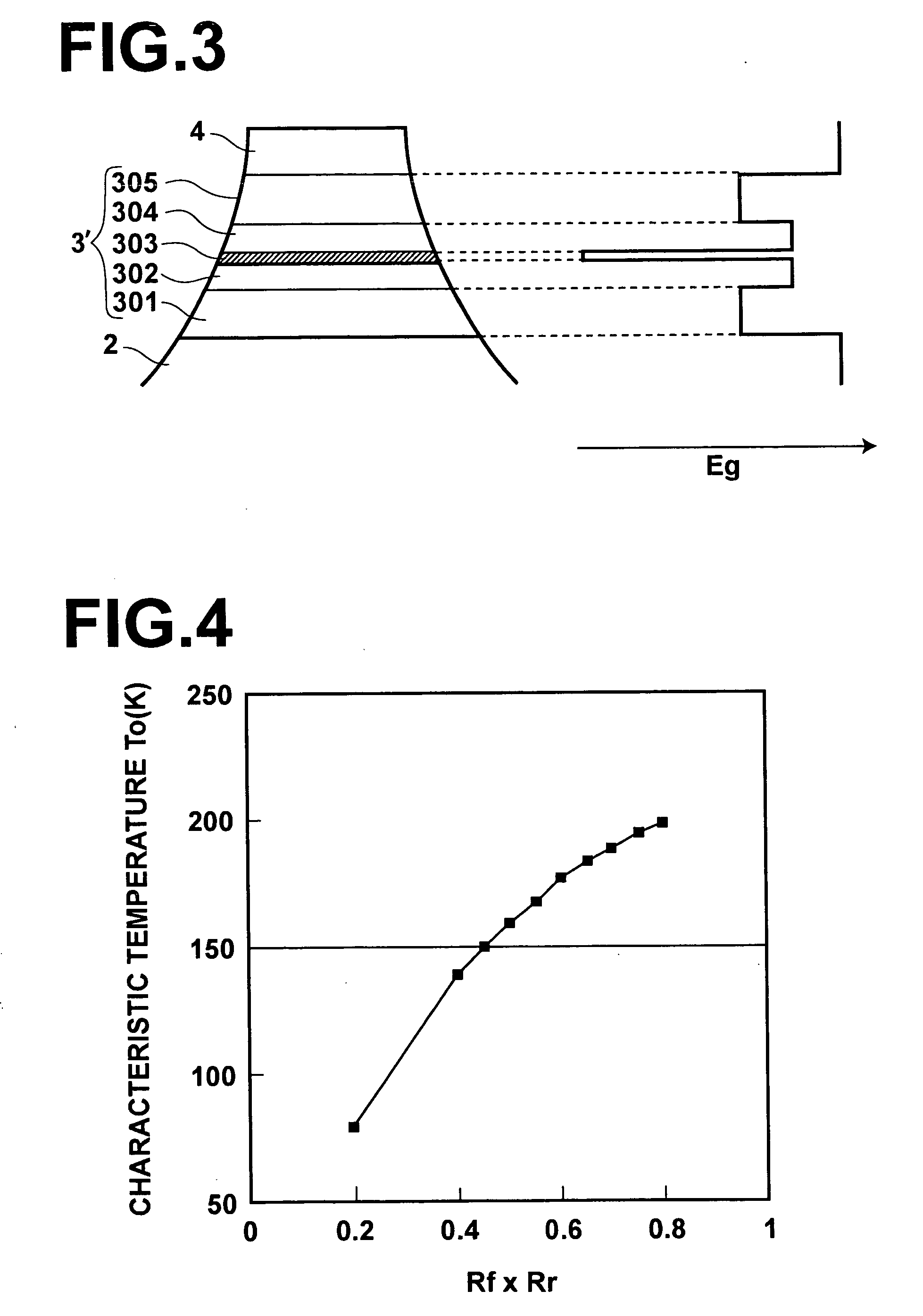
[0042]FIG. 3 is a diagram indicating details of the structure of the measured emission layer 3′ in the semiconductor laser element according to the second embodiment (in the left half of FIG. 3) and the bandgaps in the respective layers of the emission layer 3′ (in the right half of FIG. 3).

[0043] According to the second embodiment, the light-emission layer 3′ has a structure in which an n-type or i-type InGaAsP lower optical waveguide layer 301 having a thickness of 40 nm, an i-type GaAsP tensile-strain carrier-blocking layer 302 having a thickness of 10 nm and a bandgap Eg of 1.65 eV, an i-type In0.2Ga0.8As compressive-strain quantum-well active layer 303 having a thickn...

third embodiment

[0055] Although, according to the first and second embodiment, the parasitic capacitances which occur at the interfaces with the current-blocking layer are reduced by forming the pair of trenches 13 on both sides of the layered structure containing the light-emission layer 3 or 3′, the parasitic capacitances can be reduced in other manners, for example, as explained below as the third embodiment of the present invention.

[0056]FIG. 6 is a schematic perspective view of a semiconductor laser element according to the third embodiment of the present invention. As illustrated in FIG. 6, the n-type In0.49Ga0.51P lower cladding layer 2, the light-emission layer 3, the p-type In0.49Ga0.51P first upper cladding layer 4, the p-type InGaP second upper cladding layer 5, the p-type AlGaInP buried layer 6, the n-type AlGaInP current-blocking layer 7, and the p-type GaAs contact layer 8 are formed on the n-type GaAs substrate 1 in a similar manner to the first and second embodiments. However, in t...


PUM


Abstract

In a semiconductor laser element, a lower cladding layer, a lower optical waveguide layer, an InGaAs compressive-strain quantum-well active layer, an upper optical waveguide layer, and an upper cladding layer are formed in this order in a stripe-shaped region on a substrate. A current-blocking layer is formed on both sides of the compressive-strain quantum-well active layer so that the compressive-strain quantum-well active layer is sandwiched between two portions of the current-blocking layer, and trenches extending along the direction of the laser resonator are formed through the current-blocking layer. Instead of providing the trenches, the widths of the layers formed above the substrate are reduced so as to form a ridge structure.

Description

BACKGROUND OF THE INVENTION [0001] 1. Field of the Invention [0002] The present invention relates to a semiconductor laser element, and in particular to a semiconductor laser element which can be used as a light source in an information processing device. [0003] 2. Description of the Related Art [0004] The personal computers have penetrated into offices and homes, and progressed so that the processing speeds of the current personal computers are comparable to the supercomputers of tens of years past. In particular, the increase in the processing speeds of the CPUs is remarkable, and the clock frequencies of some of the currently available CPUs exceed 3 GHz. It is considered that the clock frequencies of CPUs can be increased to about 10 GHz by using only the currently known techniques. [0005] However, even when the processing speeds of the CPUs per se are increased, the substantial processing speeds of computers do not increase unless the data transfer rates between each CPU and oth...

Claims


Application Information

Patent Timeline
IPC IPC(8): H01S5/00H01S5/227H01S5/10H01S5/20H01S5/22H01S5/32H01S5/34H01S5/343
CPCB82Y20/00H01S5/0287H01S5/1039H01S5/2086H01S5/34313H01S5/2222H01S5/227H01S5/3211H01S5/3403H01S5/221
Inventor ASANO, HIDEKI
Owner FUJIFILM HLDG CORP
Why Eureka
Try Eureka