Method for forming capacitor of semiconductor device

a technology of semiconductor devices and capacitors, which is applied in the direction of capacitors, semiconductor devices, electrical devices, etc., can solve the problems of long time-consuming and laborious, inferior characteristics of capacitors having flexural electrodes, and difficulties in enabling capacitors to be used, so as to increase the effective surface area

a technology of semiconductor devices and capacitors, which is applied in the direction of capacitors, semiconductor devices, electrical devices, etc., can solve the problems of long time-consuming and laborious, inferior characteristics of capacitors having flexural electrodes, and difficulties in enabling capacitors to be used, so as to increase the effective surface area

US20050202645A1Inactive Publication Date: 2005-09-15SK HYNIX INC

Image

  • Method for forming capacitor of semiconductor device
  • Method for forming capacitor of semiconductor device
  • Method for forming capacitor of semiconductor device

Examples


Embodiment Construction

[0039] Hereinafter, a preferred embodiment of the present invention will be described with reference to the accompanying drawings. In the following description and drawings, the same reference numerals are used to designate the same or similar components, and so repetition of the description on the same or similar components will be omitted.

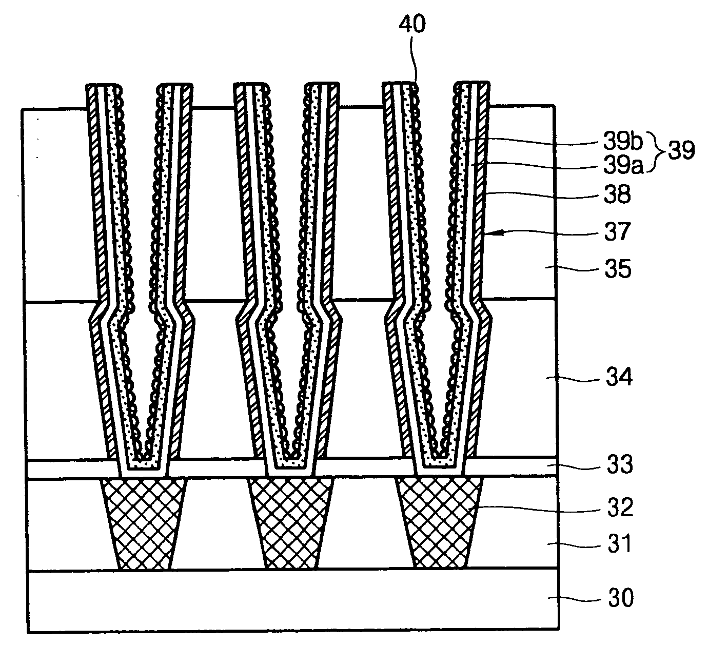
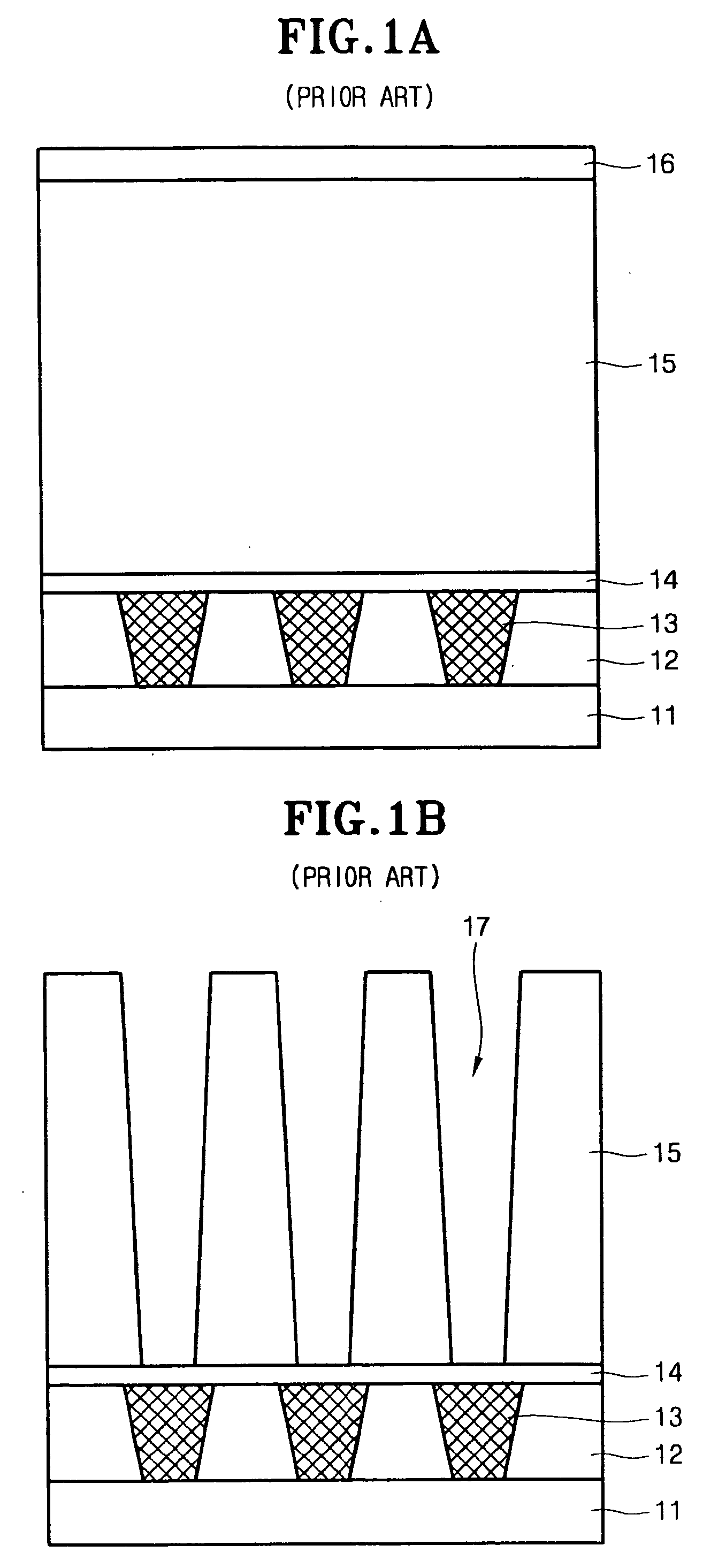
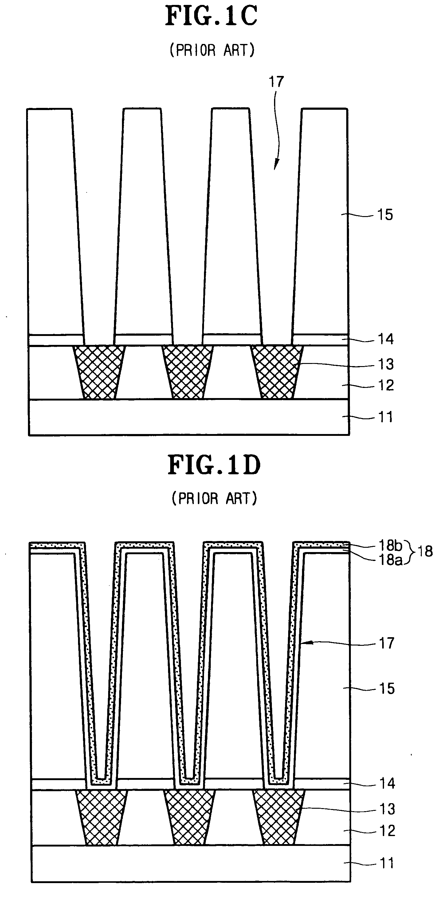
[0040]FIGS. 3a through 3h are cross-sectional views sequentially showing steps of a process of forming a capacitor according to the present invention.

[0041] In the step shown in FIG. 3a, an insulating interlayer 31 having plugs 32 is formed on a semiconductor substrate 30 according to a known process. Then, an etch stop layer 33, a first oxide layer 34, a second oxide layer 35, and a hard mask layer 36 are formed in sequence on the insulating interlayer 31 having the plugs 32.

[0042] Preferably, the etch stop layer 33 is a nitride film having a thickness of 400˜1000 Å. Also, the first oxide layer 34 is a phosphor silicate glass (PSG) film, a bo...


PUM


Abstract

Disclosed is a method for forming a capacitor of a semiconductor device. An etch stop layer, first oxide layer and second oxide layer are sequentially deposited on an insulating interlayer of a substrate. Contact holes through which portions of the etch stop layer are exposed above plugs of the insulating interlayer are formed. The contact holes are cleaned by a cleaning solution having an etching selectivity which is higher for the first oxide layer than for the second oxide layer, thereby enlarging lower portions of the contact holes. A spacer nitride layer is formed on surfaces of the contact holes and the second oxide layer. Portions of the spacer nitride layers located on the second oxide layer and above the plugs together with portions of the etch stop layer located on the plugs are removed. A double polysilicon layer is formed on the spacer nitride layer segments.

Description

BACKGROUND OF THE INVENTION [0001] 1. Field of the Invention [0002] The present invention relates to a method for forming a capacitor of a semiconductor device, and more particularly to a method for forming a capacitor of a semiconductor device, which can suppress formation of bridges between lower electrodes of the capacitor, and can improve various characteristics of the capacitor, in relation to leakage current, capacitance, and breakdown voltage of the capacitor. [0003] 2. Description of the Prior Art [0004] As generally known in the art, Dynamic RAMS (DRAMs) store data without being directly and constantly connected to power source, and so they should be refreshed at regular intervals. In other words, DRAMs store data in the form of charge on capacitors, and so require that the capacitors be recharged regularly: every few milliseconds. Further, the larger the capacitance of the capacitors is, the longer the data stored in the DRAMs can be maintained. [0005] However, a recent tr...

Claims


Application Information

Patent Timeline
15 Sep 2005
Publication
US20050202645A1
IPC
H01L21/02; H01L21/20; H01L27/108; H01L21/8238; H01L21/8242
CPC
H01L27/10852; H01L28/84; H01L28/75; H10B12/033; H10B12/00
Inventors
KIM, GYU HYUN; YOON, HYO GEUN