Semiconductor device and manufacturing method therefor

a semiconductor and manufacturing method technology, applied in the direction of organic semiconductor devices, instruments, optics, etc., can solve the problems of polysilicon films, polysilicon films, and the entire row of pixels being completely off, so as to achieve the effect of raising the reliability of a tft and effectively suppressing the deterioration due to a hot carrier

Inactive Publication Date: 2005-09-22
SEMICON ENERGY LAB CO LTD
View PDF82 Cites 51 Cited by
  • Summary
  • Abstract
  • Description
  • Claims
  • Application Information

AI Technical Summary

Benefits of technology

[0019] Further, a second characteristic of the present invention resides in that it is formed into a state in which the gate wiring (including the gate electrodes) covers (overlaps) at least a part of the LDD region, through the gate insulating film. Deterioration due to a hot carrier can also be effectively suppressed with this type of structure
[0020] In addition, a third characteristic of the present invention is that, through the multiplier effect of the first characteristic and the second characteristic described above, the reliability of a TFT can be raised.

Problems solved by technology

The driver circuit that drives all of the pixels is extremely complex, and furthermore is formed from a large number of TFTs.
If an abnormality occurs in the driver circuit, especially, this invites a fault called a line defect in which one column (or one row) of pixels turns completely off.
However, TFTs which use polysilicon films are still not equal to the MOSFETs (transistors formed on top of a single crystal semiconductor substrate), used in LSIs etc., from a reliability point of view.
As long as this shortcoming is not overcome, such a view that it is difficult to use TFTs when forming an LSI circuit gets stronger.
However, compared with a normal LDD structure, the structure published in the paper has a problem in that the off current (the current that flows when the TFT is in the off state) gets large, and therefore a countermeasure is necessary.

Method used


Image

  • Semiconductor device and manufacturing method therefor
  • Semiconductor device and manufacturing method therefor
  • Semiconductor device and manufacturing method therefor

Examples


embodiment 1

[Embodiment 1]

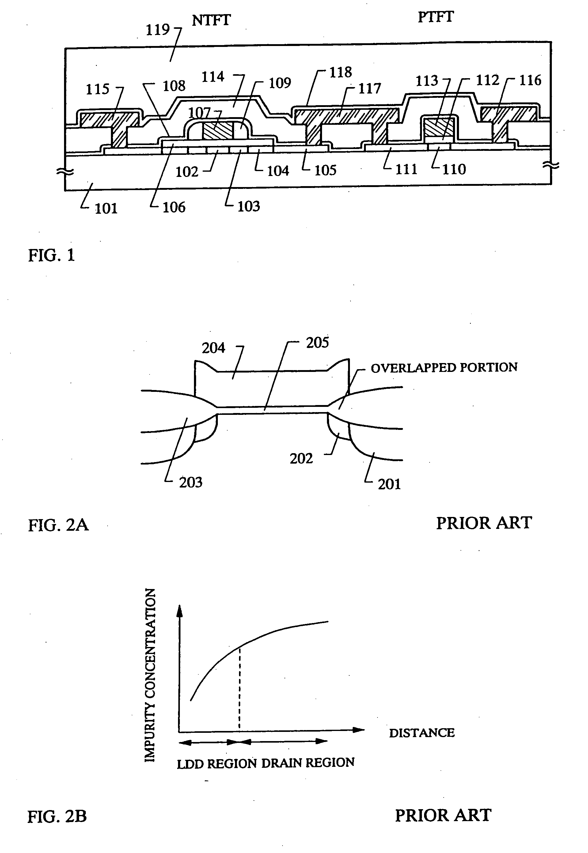
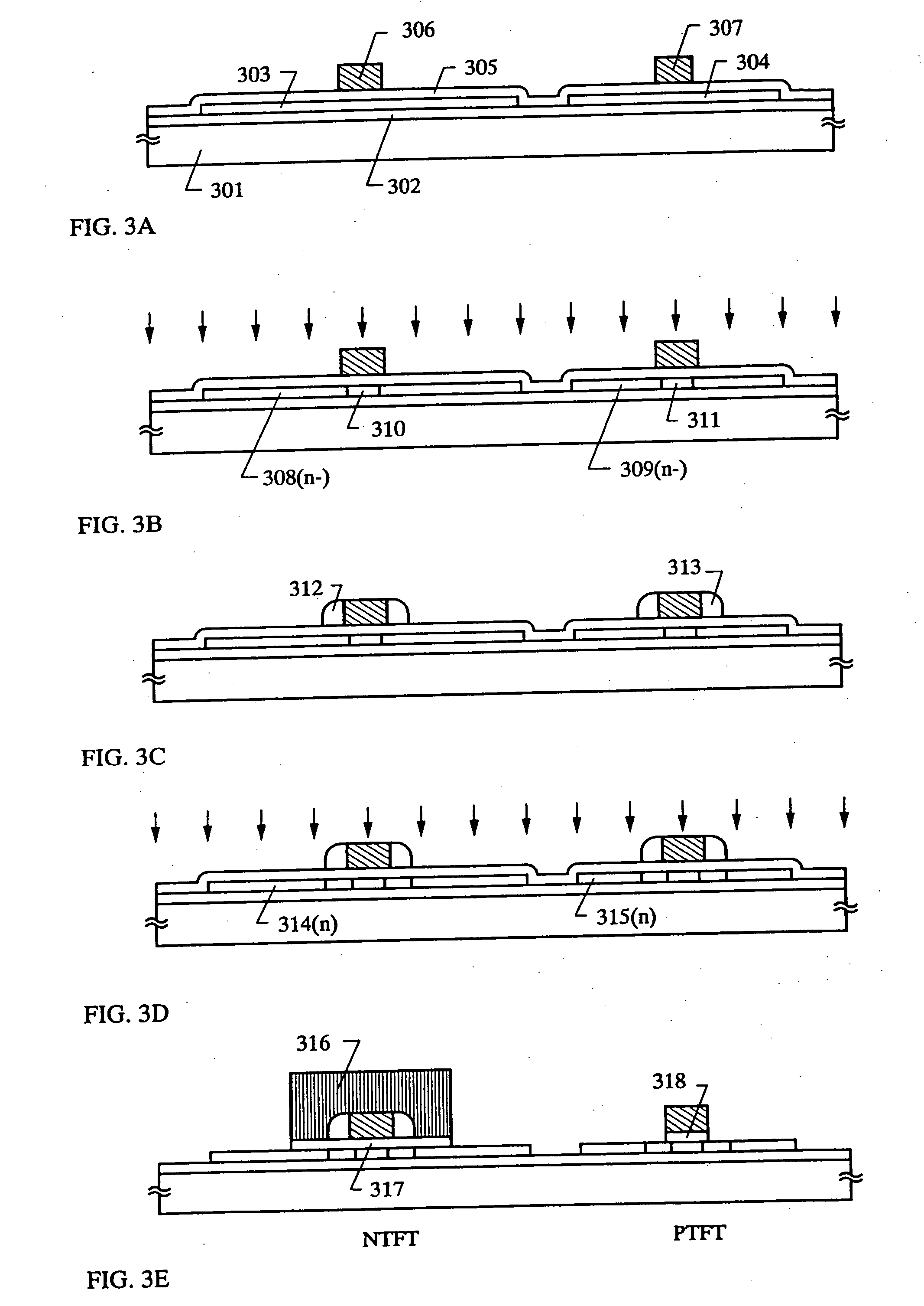
[0103] In embodiment 1, the manufacturing method of the CMOS circuit shown in FIG. 1 is explained using FIGS. 3A to 3E, FIGS. 4A to 4D, and FIGS. 5A-5B.

[0104] First, a 200 nm silicon oxide film 302 that becomes a base film is formed on a glass substrate 301. It may laminate a silicon nitride film onto the base film, and may use only a silicon nitride film. Plasma CVD, thermal CVD, or sputtering may be used as a film deposition method. Of course, doping boron into the silicon nitride film is effective to increase the radiation effect.

[0105] Next, a 50 nm amorphous silicon film is formed by plasma CVD, thermal CVD, or sputtering, on the silicon oxide film 302. Crystallization of the amorphous silicon film is carried out afterward by using the technique disclosed in Japanese Patent Application Laid-open No. Hei 7-130652, forming a semiconductor film containing crystals. This process is explained using FIGS. 5A and 5B.

[0106] First, a silicon oxide film 502 is formed as ...

embodiment 2

[Embodiment 2]

[0144] Undoped Si (an intrinsic silicon layer or an undoped silicon layer), in which impurities are intentionally not doped, is used in embodiment 1 for the sidewalls. However, in embodiment 2, a phosphorous doped silicon layer (“n+”-Si layer), in which phosphorous is doped during film formation, or a boron doped silicon layer (“p+”-Si layer) is used. It is needless to say that the silicon layer may be amorphous, non-crystalline, or micro-crystalline.

[0145] By using a silicon layer doped with phosphorous or boron, the entire sidewall portion is made low resistance, and the possible change in characteristics originating in fluctuation of the phosphorous concentration profile can be eliminated, which is the fear of process shown in FIG. 3D.

embodiment 3

[Embodiment 3]

[0146] Undoped Si (an intrinsic silicon layer or an undoped silicon layer), in which impurities are intentionally not doped, is used in embodiment 1 for the sidewalls. However, in embodiment 3, a silicon layer that contains either of carbon (C), nitrogen (N), or oxygen (O) is used, to thereby increase the resistive component of the sidewalls. Of course, the silicon layer may be either amorphous, crystalline, or micro-crystalline. Further, oxygen is best as the impurity to be used.

[0147] Namely, it may only dope with carbon, nitrogen, or oxygen at 1 to 50 atomic % (typically, from 10 to 30 atomic %) when forming the silicon layer that becomes the sidewalls. Oxygen at 20 atomic % is doped in this embodiment 3.

[0148] With employing the structure of embodiment 3, the resistive component due to the sidewalls becomes larger. Accordingly, it may take such a structure that the capacitive component in which the sidewalls act as the dielectric in response to the applied gate v...


PUM

PropertyMeasurementUnit
lengthaaaaaaaaaa
lengthaaaaaaaaaa
lengthaaaaaaaaaa

Abstract

An active layer of an NTFT includes a channel forming region, at least a first impurity region, at least a second impurity region and at least a third impurity region therein. Concentrations of an impurity in each of the first, second and third impurity regions increase as distances from the channel forming region become longer. The first impurity region is formed to be overlapped with a side wall. A gate overlapping structure can be realized with the side wall functioning as an electrode.

Description

BACKGROUND OF THE INVENTION [0001] 1. Field of the Invention [0002] The present invention relates to a semiconductor device having circuits structured with thin film transistors (hereinafter referred to as TFT). For example, the present invention relates to electro-optical devices, typically liquid crystal display panels, and to the structure of electronic equipments loaded with such electro-optical devices as parts. Note that throughout this specification semiconductor device generally indicates devices that acquire their function through the use of semiconductor characteristics, and electro-optical devices, semiconductor circuits, as well as electronic equipments are semiconductor devices. [0003] 2. Description of the Related Art [0004] Active matrix type liquid crystal display devices composed of TFT circuits that use polysilicon films have been in the spotlight in recent years. They are the backbone for realizing high definition image displays, in which a plurality of pixels are...

Claims


Application Information

Patent Timeline
Patent Type & Authority Applications(United States)
IPC IPC(8): G02F1/1362H01L21/77H01L21/84H01L27/12H01L27/32H01L29/04H01L29/786H01L51/52
CPCG02F1/13454H01L27/12H01L27/3244H01L27/3246H01L27/3248H01L27/3262H01L27/1277H01L29/78627H01L29/78645H01L51/5246H01L51/5284H01L2251/5315H01L2029/7863H01L29/78621H10K59/122H10K59/12H10K59/123H10K59/1213H10K50/8426H10K50/865H10K2102/3026
Inventor YAMAZAKI, SHUNPEIOHTANI, HISASHIHAMATANI, TOSHIJI
Owner SEMICON ENERGY LAB CO LTD
Why Eureka
Try Eureka