

Method for manufacturing gratings in semiconductor materials that readily oxidise
a technology of semiconductor materials and manufacturing methods, applied in semiconductor lasers, instruments, optical elements, etc., can solve the problems of index-coupled lasers sensitive to perturbation, inability to control this phenomenon, and heavily influenced performance of these lasers, etc., and achieve the effect of oxidizing quickly
- Summary
- Abstract
- Description
- Claims
- Application Information
AI Technical Summary
Benefits of technology
Problems solved by technology
Method used
Image

Examples
Embodiment Construction
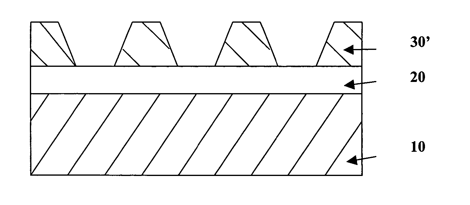
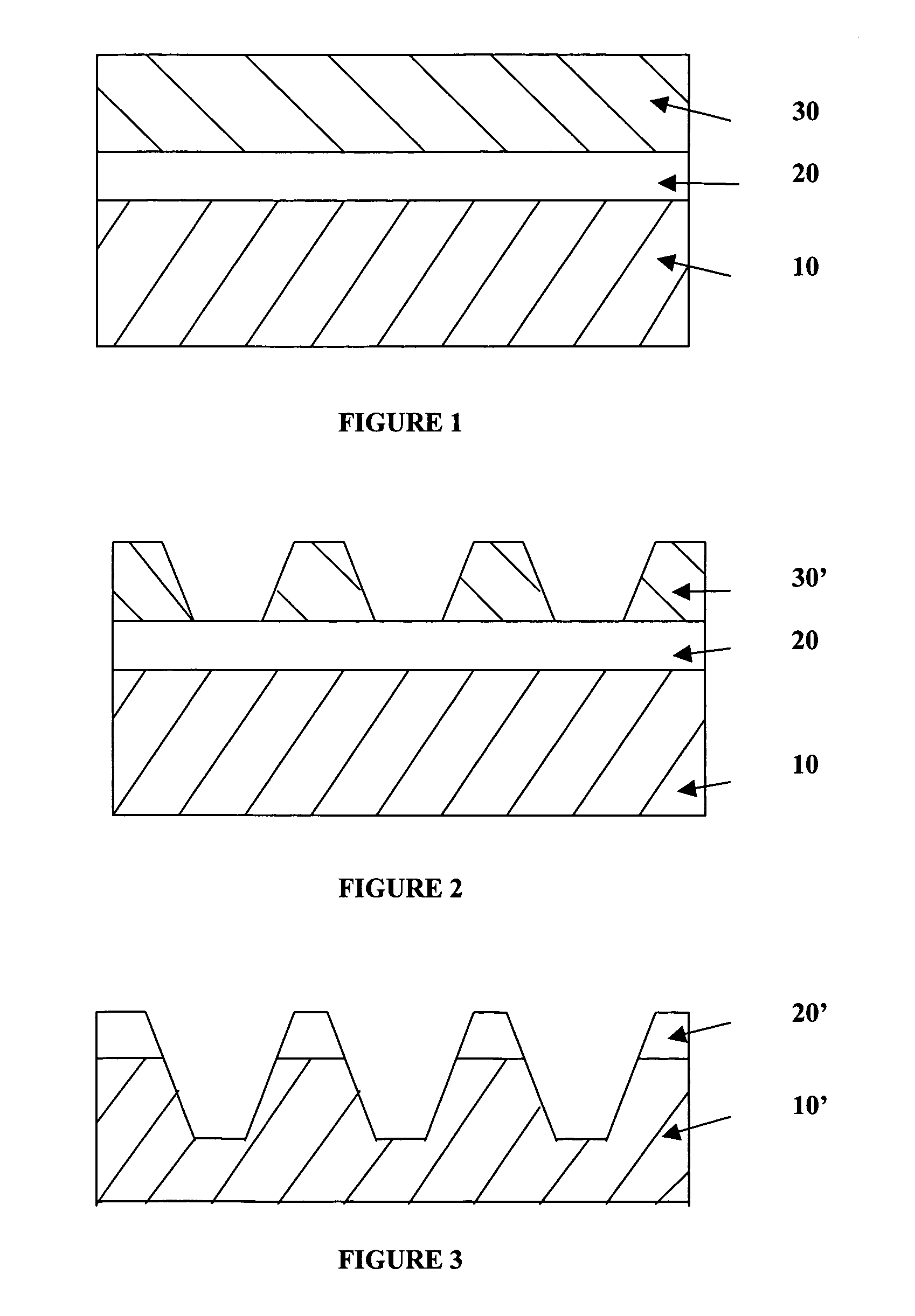
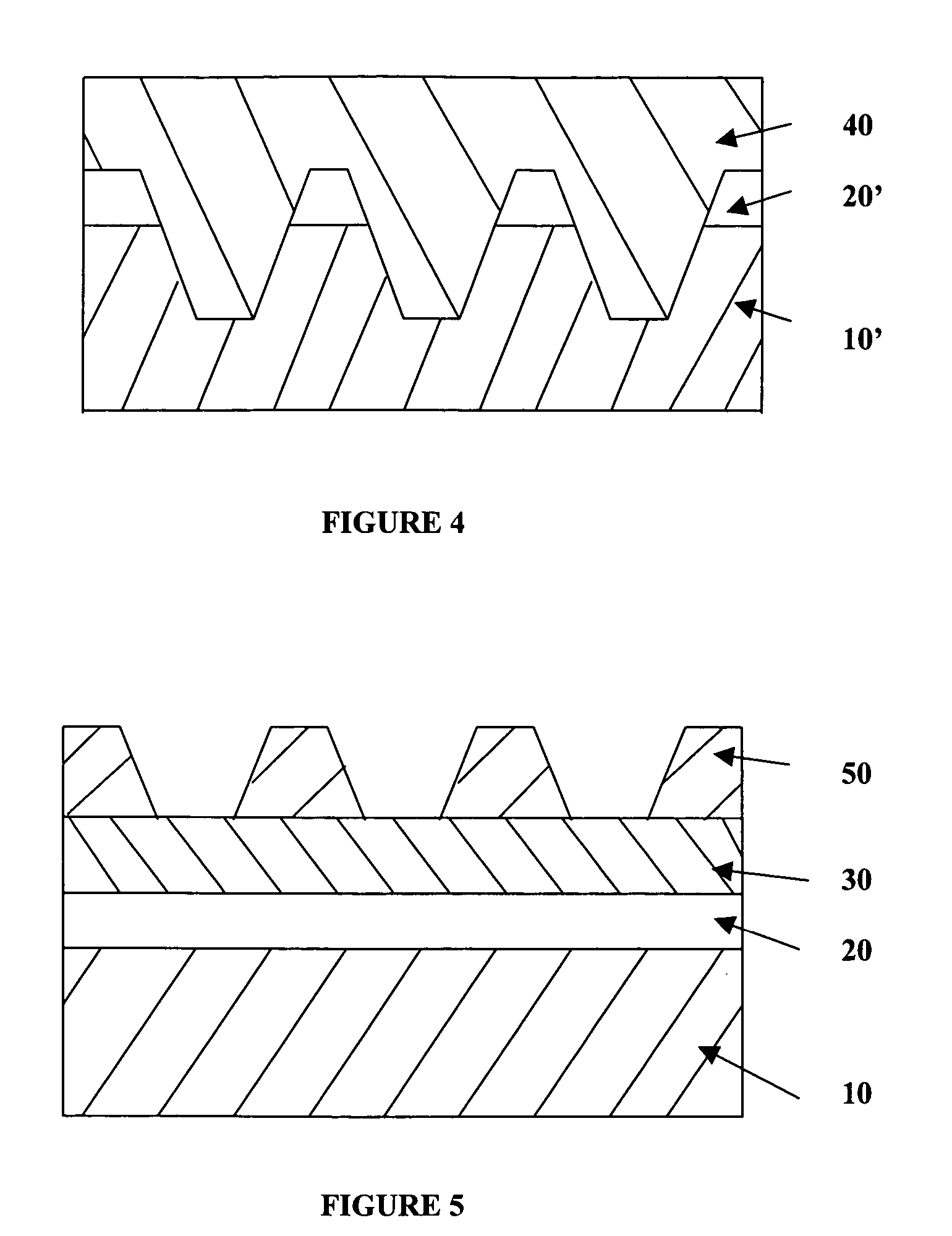
[0023] The present invention provides a method of manufacturing gratings in semiconductor material that readily oxidises. The method is suitable for a wide range of applications, and is particularly appropriate for fabricating gratings for distributed feedback lasers, gratings for distributed Bragg reflectors, and filters based on optical waveguides with grating structures, for example. The invention provides an improved accuracy of the grating depth and shape, and a reduction in contaminants and oxidants within the gratings etched into the semiconductor material that readily oxidises, with consequent improved performance and manufacturing repeatability thereof, for example.
[0024] The present invention is a combination of in-situ etching with a grating mask pattern comprised only of semiconductor material, together with the fabrication of a protective layer beneath the semiconductor grating mask that protects the semiconductor material that readily oxidises. As such the present inv...
PUM
| Property | Measurement | Unit |
|---|---|---|
| compositions | aaaaa | aaaaa |
| temperatures | aaaaa | aaaaa |
| threshold current | aaaaa | aaaaa |
Abstract
Description
Claims
Application Information