
Memory devices based on electric field programmable films

a technology of programmable films and memory devices, applied in thermoelectric devices, instruments, nanoinformatics, etc., can solve the problems of high fabrication cost, high power consumption, complex architecture,

Inactive Publication Date: 2005-09-29
BU LUJIA +4
View PDF7 Cites 61 Cited by
  • Summary
  • Abstract
  • Description
  • Claims
  • Application Information

AI Technical Summary

Benefits of technology

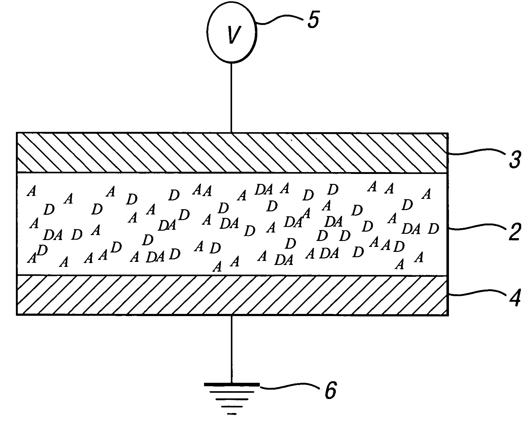
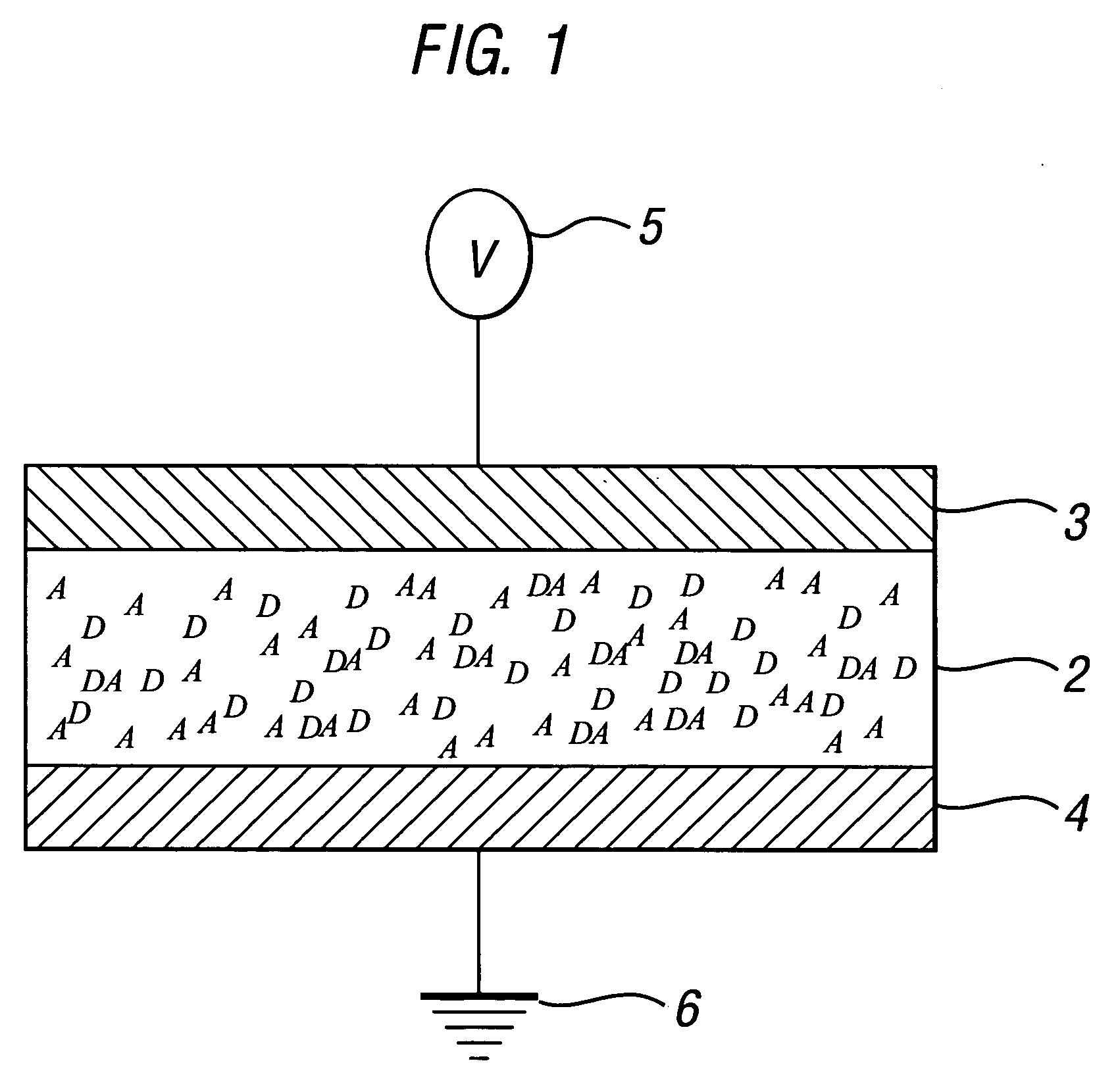
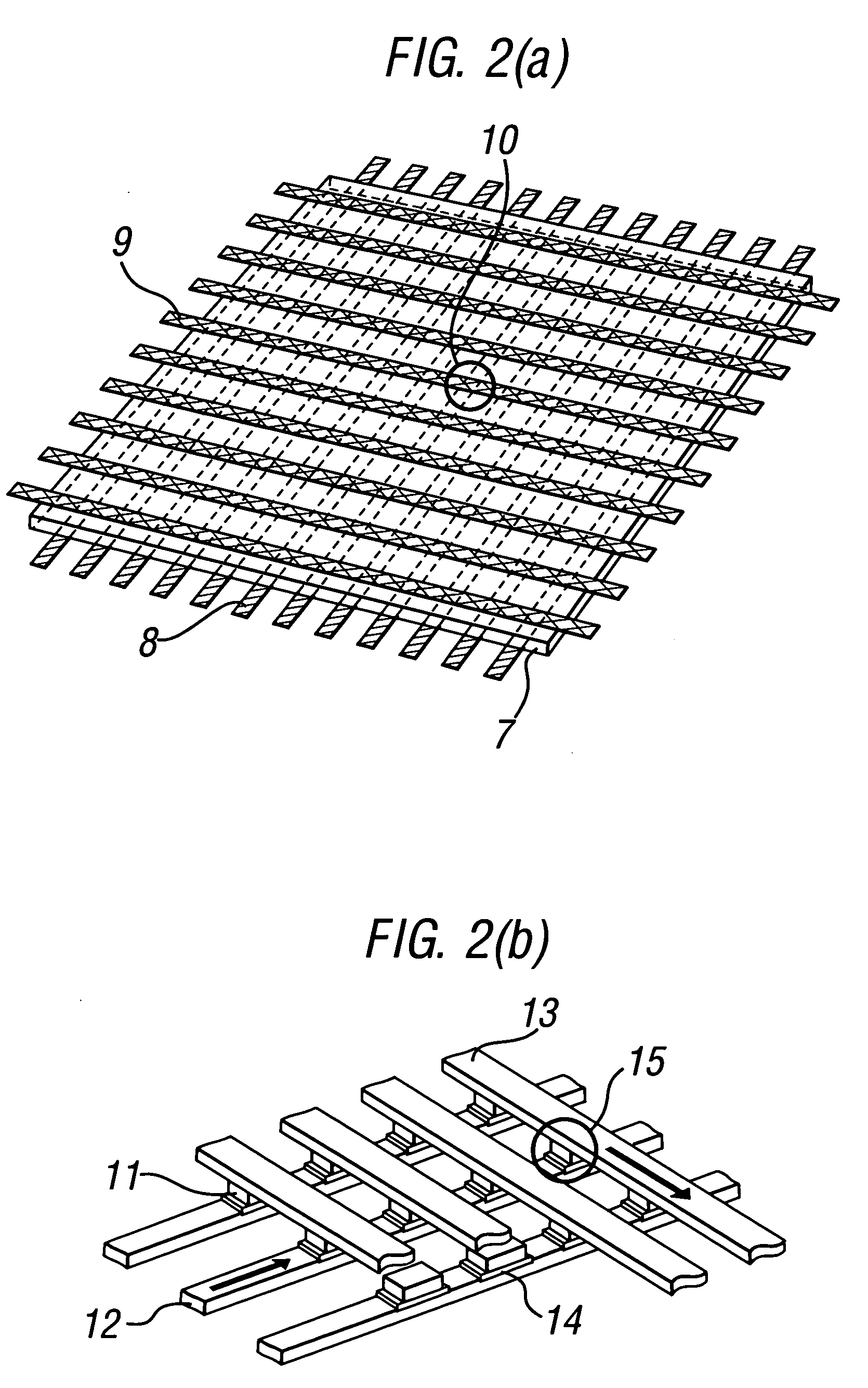
"The patent describes an electric field programmable film that can be used in data processing machines and memory devices. The film is made by depositing a composition of a polymer and an electroactive moiety onto a substrate. The film can be programmed to change its state by applying an electric field, making it a useful tool for data processing. The technical effect of this patent is the creation of a versatile and programmable film that can be used in various electronic devices."

Problems solved by technology

Although these devices have been technically and commercially successful, they have a number of drawbacks, including complex architectures and high fabrication costs.
This results in heating and high power consumption.
Non-volatile semiconductor devices avoid this problem but have reduced data storage capability as a result of higher complexity in the circuit design, which consequently results in higher production costs.
However, many currently known bistable films are inhomogeneous, multilayered composite structures fabricated by evaporative methods, which are expensive and can be difficult to control.
In addition, these bistable films do not afford the opportunity for fabricating films in topographies ranging from conformal to planar.
Bistable films fabricated using polymer matrices and particulate matter are generally inhomogeneous and therefore unsuitable for fabricating submicrometer and nanometer-scale electronic memory and switching devices.
Still other bistable films can be controllably manufactured by standard industrial methods, but their operation requires high temperature melting and annealing at the grid intersection points.
Such films generally suffer from thermal management problems, have high power consumption requirements, and afford only a small degree of differentiation between the “conductive” and “nonconductive” states.
Furthermore, because such films operate at high temperatures, it is difficult to design stacked device structures that allow high density memory storage.

Method used


Image

  • Memory devices based on electric field programmable films
  • Memory devices based on electric field programmable films
  • Memory devices based on electric field programmable films

Examples


example 1

[0136] This example demonstrates the synthesis of gold nanoparticles used as electron donors. Gold nanoparticles were synthesized at room temperature using a two-phase arrested growth method detailed by M. J. Hostetler, et. al., Langmuir, 14 (1998) 17. In a typical synthesis, an aqueous solution containing 0.794 grams (g) (2 millimole (mmol)) of tetrachloroauric acid (HAuCl4.3H2O), in 50 milliliters (ml) of water was added to an 80 ml toluene solution containing 3.0 g (5.5 mmol) of tetraoctylammonium bromide. The mixture was stirred vigorously for 1 hour. To the separated toluene solution was added 0.81 g (4 mmol) of dodecane thiol (DSH). The resulting mixture was stirred for 10 minutes at room temperature. A 50 ml aqueous solution of sodium tetrahydridoborate (NaBH4) (20 mmol) was then added to the mixture over a 10 second period with vigorous stirring and the resulting mixture was further stirred for 1 hour at room temperature. The dark colored toluene phase was collected, washed ...

examples 2-18

[0137] Different sized nanoparticles were obtained by varying the temperature of reduction during the addition of NaBH4 solution and subsequent stirring. Different sized nanoparticles were also obtained by varying the addition time of the NaBH4 solution or the molar ratio of DSH to HAuCl4.3H2O. Results are summarized in Table 2 below.

TABLE 2NaBH4radiusDSH / AuTemperatureaddition timeof gyrationExampleMolar ratio(° C.)(sec)(nm)20.220101.731.120101.2942202551.3652205001.3762205001.417255101.3282552061.3590.2552061.95101.28555001.3411290101.34120.290102.16131.190101.44141.1902551.39150.2205001.99160.2905002.73172905001.33182902551.31

example 19

[0138] This example demonstrates the synthesis of 9-anthracenemethyl methacrylate. A two liter, 3-necked round bottomed flask was equipped with a condenser, dropping addition funnel, mechanical stirrer, and gas inlet tube. The flask was charged with 9-anthracenemethanol (48.9 grams, 0.235 mol) and purged with nitrogen for 10 minutes. Anhydrous tetrahydrofuran (300 ml), pyridine (33 mL), and triethylamine (50 mL) were added to the flask, and the resulting solution was cooled to 0° C. Methacryloyl chloride (technical grade, 37.5 ml, 40.1 grams, 0.345 mol) was added using a syringe into the addition funnel, and added slowly dropwise to the vigorously stirring solution over the course of 1 hour. A brownish precipitate formed and aggregated into a gummy mass, which periodically interfered with stirring. The reaction was kept at a temperature of 0° C. for 2 hours and was then allowed to gradually warm up to room temperature overnight. The reaction was quenched with water (400 ml). Ethyl e...


PUM

PropertyMeasurementUnit
thicknessaaaaaaaaaa
dielectric constantaaaaaaaaaa
wavelengthaaaaaaaaaa

Abstract

Disclosed herein is an electric field programmable film comprising a polymer bonded to an electroactive moiety. Disclosed herein too is a method of manufacturing an electric field programmable film comprising depositing upon a substrate, a composition comprising a polymer and an electroactive moiety that is bonded to the polymer. Disclosed herein too is a data processing machine comprising a processor for executing an instruction; and a memory device comprising an electric field programmable film, wherein the electric field programmable film comprises a polymer bonded to an electroactive moiety, and further wherein the memory device is in electrical and / or optical communication with the processor.

Description

BACKGROUND OF THE INVENTION [0001] The present disclosure relates to electronic memory devices based on electric field programmable films. [0002] Electronic memory and switching devices are presently made from inorganic materials such as crystalline silicon. Although these devices have been technically and commercially successful, they have a number of drawbacks, including complex architectures and high fabrication costs. In the case of volatile semiconductor memory devices, the circuitry must constantly be supplied with a current in order to maintain the stored information. This results in heating and high power consumption. Non-volatile semiconductor devices avoid this problem but have reduced data storage capability as a result of higher complexity in the circuit design, which consequently results in higher production costs. [0003] Alternative electronic memory and switching devices employ a bistable element that can be converted between a high impedance state and a low impedance...

Claims


Application Information

Patent Timeline
Patent Type & Authority Applications(United States)
IPC IPC(8): C08J5/18C08G85/00C08K3/00C08L101/00G11C11/56G11C13/02H01L27/10H01L29/08H10K99/00
CPCB82Y10/00G11C11/5664G11C13/0009G11C13/0014G11C13/0016H01L51/0595G11C2213/72G11C2213/77H01L27/285H01L51/0032G11C2213/71H10K19/202H10K85/00H10K10/701
Inventor BU, LUJIACAGIN, EMINECUTLER, CHANDRAGRONBECK, DANA A.SZMANDA, CHARLES R.
Owner BU LUJIA
Learn More