Demodulator circuit, radio communication system and communication semiconductor integrated circuit

a demodulator circuit and integrated circuit technology, applied in multiplex communication, orthogonal multiplex, baseband system details, etc., can solve the problems of long period, inability to precisely correct transmission path response, and noise component to appear as error in the estimation of transmission path response, so as to reduce delay time, reduce the time taken for gain control, and suppress circuit scale from increasing

Inactive Publication Date: 2005-09-29
RENESAS TECH CORP
View PDF8 Cites 50 Cited by
  • Summary
  • Abstract
  • Description
  • Claims
  • Application Information

AI Technical Summary

Benefits of technology

[0019] According to the invention of this application, there is also provided a demodulator circuit having gain adjusting means for adjusting the gain to the received signal, A/d converter means for converting the received analog signal adjusted in gain to a digital signal, a finite impulse response type filter (FIR filter) for removing the out-of-band component signal from the received digital signal, and an auto gain control for automatically controlling the FIR filter output by using the gain adjusting means, so that the stage number of the FIR filter can be changed by switching before and after of the gain control. By this construction to change the filter stage number, it is possible to decrease the stage number of the FIR filter at the time of automatic gain control, and hence reduce the delay time. Thus, the time taken for the gain control can be shortened.
[0020] Furthermore, according to the invention of this application, a fast Fourier transform (F

Problems solved by technology

At this time, since the received packet normally contains both transmission path response and noise, a simple comparison with the known preamble pattern will cause the noise component to appear as error in the estimation of the transmission path response

Method used


Image

  • Demodulator circuit, radio communication system and communication semiconductor integrated circuit
  • Demodulator circuit, radio communication system and communication semiconductor integrated circuit
  • Demodulator circuit, radio communication system and communication semiconductor integrated circuit

Examples


embodiment 1

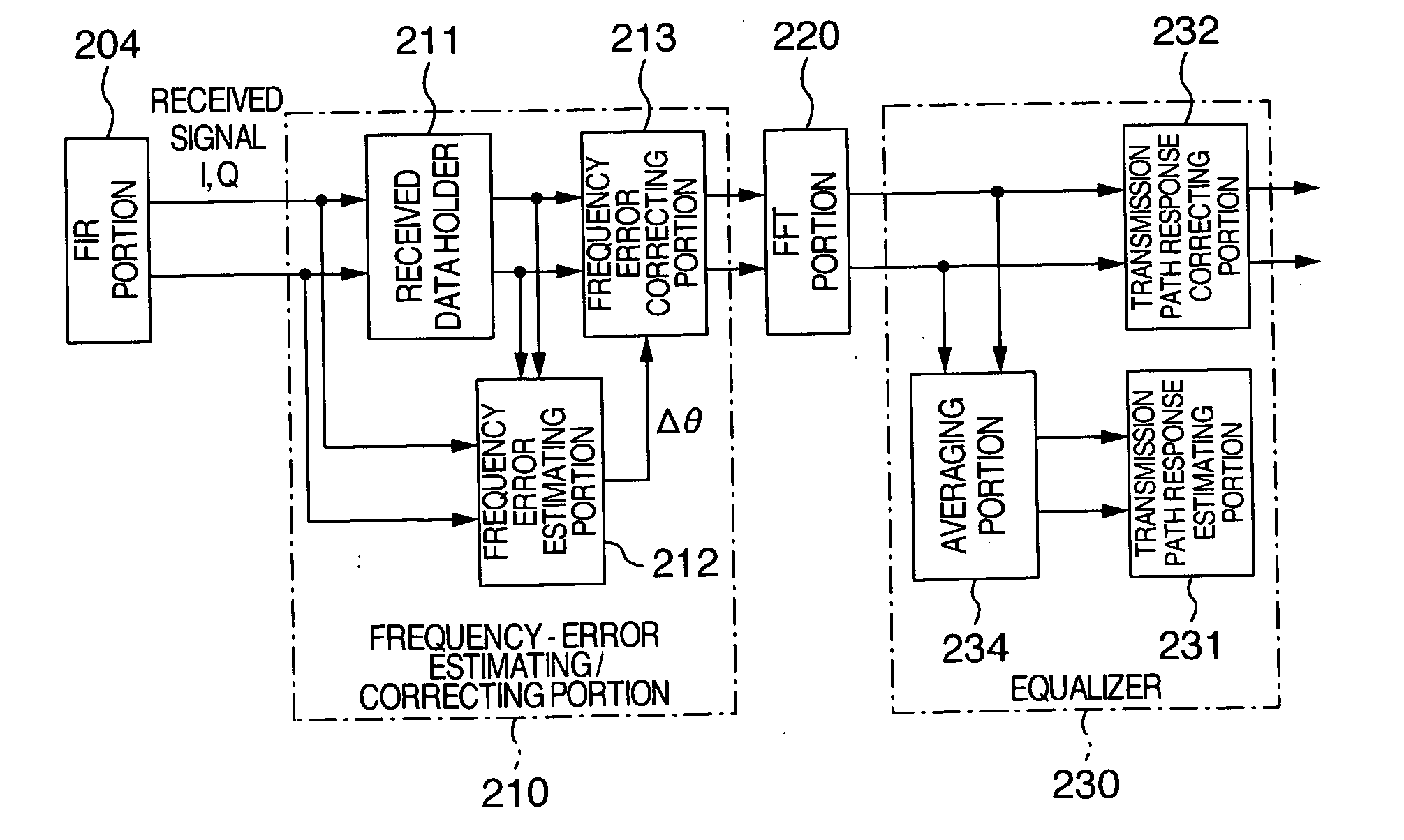
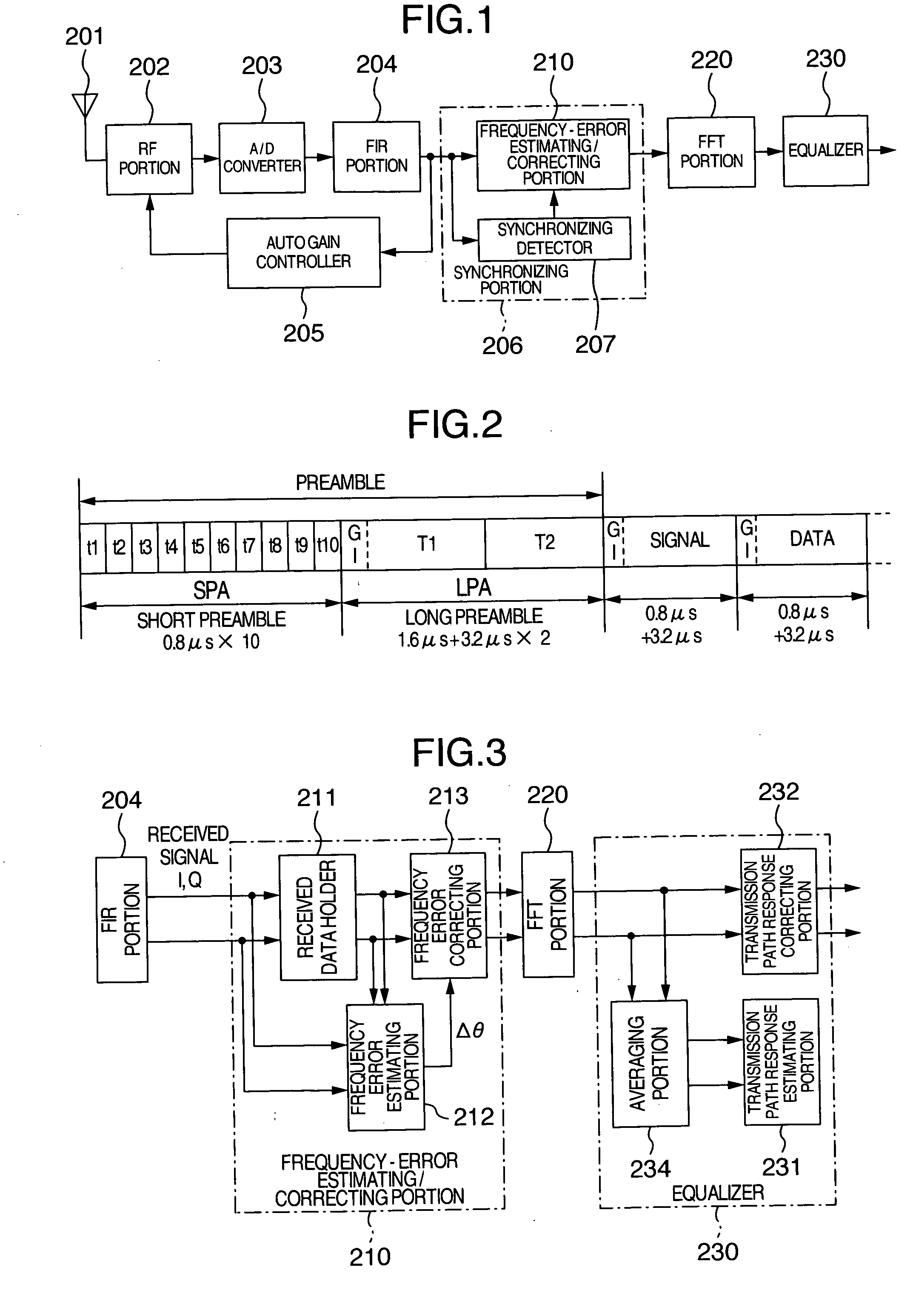
[0048]FIG. 4 shows the first embodiment of the OFDM demodulator circuit. The OFDM demodulator circuit of this embodiment has, as does the OFDM demodulator circuit examined by the inventors before this invention, the FIR filter 204 that removes the out-of-band high-frequency components from the received and A / D-converted signals I and Q, the frequency error estimating / correcting portion 210 that estimates and corrects for the frequency error, the FFT portion 220 that converts the received signal from the time-axis information to the frequency-axis information, and the equalizer 230 that estimates and corrects the transmission path response by comparing the preamble pattern of the received packet converted to the frequency-axis information and a known preamble pattern.

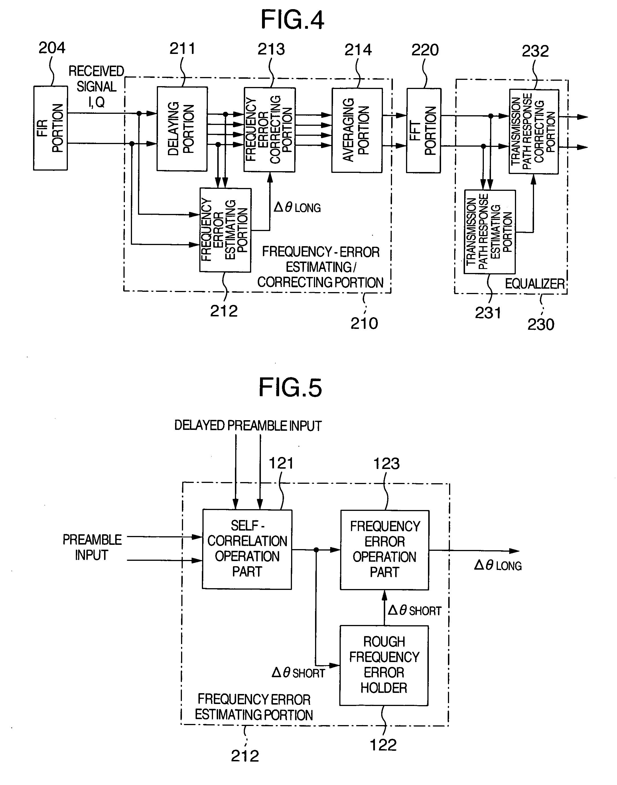
[0049] The frequency error estimating / correcting unit 210 has the delaying portion 211 that is formed of delay elements and that delays the short preamble of the received packet by a period of 16 samples, the frequency ...

embodiment 2

[0087]FIG. 12 shows the second embodiment of the OFDM demodulator circuit according to the invention. In this embodiment, the frequency-error estimating / correcting portion 210 has another delaying portion 215 in addition to the delaying portion 211 for holding the short preamble or long preamble for frequency error estimation. This delaying portion 215 is used to delay the long preamble after correction in order that the long preamble can be averaged. The operations up to the output of frequency-error estimate are the same as in the embodiment 1, and thus will not be described. The frequency-error correcting portion 213 is constructed as shown in FIG. 13. From the comparison with the construction of frequency-error correcting portion 213 of the embodiment 1 shown in FIG. 7, it will be apparent that a single complex multiplier is used in this embodiment.

[0088] In addition, while the frequency-error correction value operation part 131 in the embodiment 1 is required to find the frequ...

embodiment 3

[0091]FIG. 15 shows an example of the construction of the FIR portion used in the third embodiment of the OFDM demodulator circuit according to the invention. FIG. 16 shows an example of the construction of a system that has the OFDM demodulator circuit including this FIR portion provided as the demodulator of the wireless LAN.

[0092] The FIR portion 204 in this embodiment, as illustrated in FIG. 15, has a filter 410 for received signal I, and a filter 420 for received signal Q. Each filter has a delay stage formed of a plurality of (n) delay elements 461a˜461n connected in series, a multiplier portion formed of multipliers 462a˜462n provided in association with the respective delay elements in order to multiply the delayed signals by predetermined coefficients a1˜an, and an adder 470 for adding the outputs from the multipliers 462a˜462n. In addition, the FIR portion 204 of this embodiment has a selector 481 provided between the m-th delay element 461b and the (m+1)-th delay element...


PUM


Abstract

A communication semiconductor integrated circuit has a demodulator circuit built in a single semiconductor chip. The demodulator circuit is constructed to demodulate a received OFDM-modulated packet signal including a preamble that has two or more fixed-signal sequences, and to have a frequency-error estimating/correcting function that estimates the frequency error of the received signal by using the received preamble and corrects the received signal for the frequency error, a fast Fourier transform function (FFT portion 210) that converts the time-axis information of the corrected received signal to frequency-axis information, a transmission path response estimating/correcting function that estimates the status of the transmission path from the converted signal and corrects the received signal for the transmission path response, and an averaging function that averages the received signal after being corrected for the frequency error so that the averaging can be performed before the fast Fourier transform process.

Description

INCORPORATION BY REFERENCE [0001] The present application claims priority from Japanese application JP2004-065567 filed on Mar. 9, 2004, the content of which is hereby incorporated by reference into this application. BACKGROUND OF THE INVENTION [0002] The present invention relates to a modulator circuit and radio communication system using the OFDM (Orthogonal Frequency Division Multiplexing) modulation system, and particularly to a technique useful for shortening the receiving process delay. [0003] There is now a modulation system using OFDM as one of the modulation systems for the transmitted signal in radio communication and digital broadcasting. Since the OFDM modulation system is a digital modulation system using a plurality of carriers that has orthogonality, it generally has excellent characteristics against multipath interference. However, since it causes a large signal distortion due to frequency error because of using a plurality of carriers, it is necessary to synchronize...

Claims


Application Information

Patent Timeline
IPC IPC(8): H04J11/00H04L25/02H04L27/00H04L27/14H04L27/26H04L27/38
CPCH04L25/022H04L25/0228H04L27/2657H04L27/3809H04L27/2675H04L2027/0048H04L2027/0065H04L2027/0095H04L27/265H04L2027/003
Inventor MATSUDA, KEISUKEOKUBO, TAKASHIHORI, TOYOKAZUTAKADA, KAZUYUKI
Owner RENESAS TECH CORP
Why Eureka
Try Eureka