Connection arrangement for optical communication systems

a technology of optical communication and connection arrangement, applied in the direction of coupling device connection, instruments, electrical apparatus, etc., can solve the problems of low cost and/or small dimension requirements imposed on the apparatus, significant problems, compatibility (emc), rf management and signal integrity, etc., to achieve easy production, reduce the influence of these fields, and facilitate the effect of production

Inactive Publication Date: 2005-09-29
AVAGO TECH WIRELESS IP SINGAPORE PTE
View PDF7 Cites 5 Cited by
  • Summary
  • Abstract
  • Description
  • Claims
  • Application Information

AI Technical Summary

Benefits of technology

[0013] A preferred embodiment of the invention is thus based on the use of a lead frame in conjunction with electromagnetic absorber material. Electrical connection of the OSAs and the ESA is ensured by means of metallic leads. These leads are easy to produce while simultaneously easy and fast to solder to the ESA.
[0014] As indicated, crosstalk and other problems related to EMC and EMI are primarily related to emissions of electromagnetic fields from the leads and / or to electromagnetic fields picked up by the leads. More specifically, crosstalk is due to the electromagnetic field irradiated from the transmitter (receiver) and picked up by the receiver (transmitter). The influence of these fields is drastically reduced by the absorber material. Using the absorber material on both the receiver (RX) and the transmitter (TX) side will drastically reduce electromagnetic emissions. Due to the absorbing properties of the material, these electromagnetic emissions are converted into thermal power, which is easily dissipated.
[0015] Additionally, the absorber material reduces the discontinuity in the electrical path generated when leads in air are used as well as the relative difference of characteristic impedance of the lead zone. The absorber material has a dielectric constant higher than air and thus closer to the dielectric constant of the PCB and the feed throughs of the OSAs.
[0016] RF-performance of the interconnection will be improved using the absorber, because the dielectric constant of the material is highly beneficial in reaching the desired characteristic impedance. Without an absorber material, a frame comprised of leads in air will typically have an impedance higher than the desired impedance. At least partly embedding the leads in an absorber material reduces the impedance and thus leads to improved performance.

Problems solved by technology

Additionally, at very high operational speeds, low cost and / or small dimension requirements imposed on apparatus give rise to significant problems in terms of electromagnetic immunity (EMI), electromagnetic compatibility (EMC), RF management and signal integrity.
However, implementing this solution is time consuming in view of the need of attaching the flex to the ESA and the OSA.
Moreover, the flex is not self-protected from crosstalk (X-Talk) and is not exempt from EMC problems.

Method used


Image

  • Connection arrangement for optical communication systems
  • Connection arrangement for optical communication systems
  • Connection arrangement for optical communication systems

Examples


Embodiment Construction

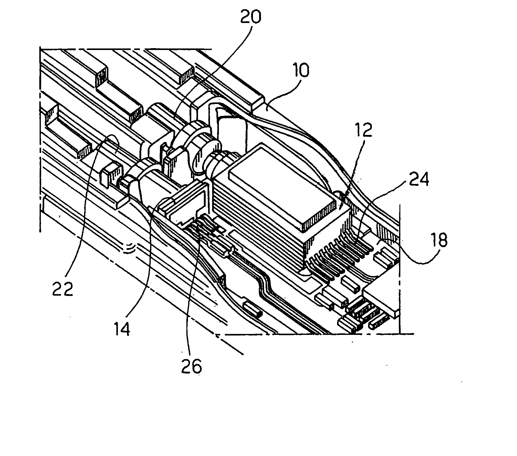
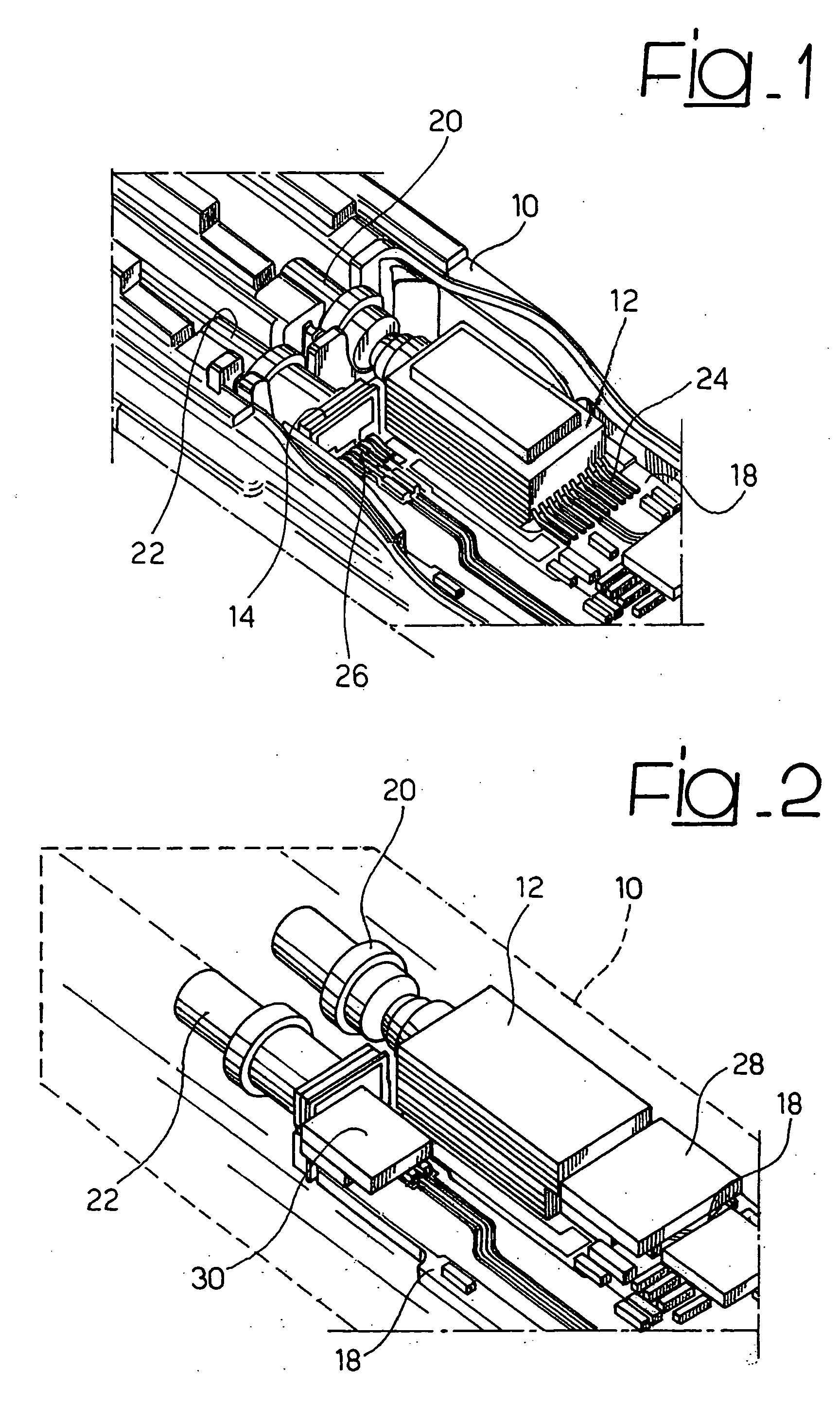
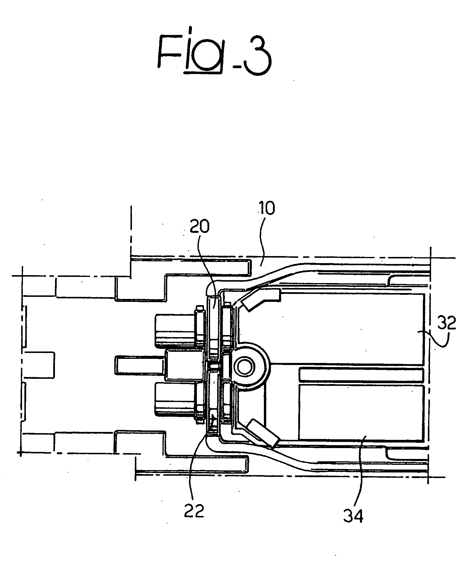
[0022] As used herein “electromagnetic absorber material” will indicate any material exhibiting the capability of absorbing electromagnetic fields / waves. More specifically, electromagnetic fields / waves in the typical ranges of interest for fiber optic communications (i.e. 30 MHz to 20 GHz) will be primarily considered. More to the point, electrically non-conductive (i.e. insulating) absorber materials will be considered.

[0023] Such materials are currently available for use as free space absorbers, cavity resonance absorbers or load absorbers in microwave products. Typical formulations include magnetically loaded, flexible silicone or urethane sheets. Alternative arrangements include variations in the loading material, such as e.g. iron loaded, ferrite loaded or dielectrically loaded materials (which may exhibit resonant properties) and / or variations in the sheet structure, such as e.g. multilayered, carbon impregnated polyurethane foam sheets, open cell foam sheets with controlled ...


PUM


Abstract

An arrangement including: an electrical subassembly, an optical subassembly, the electrical subassembly and the optical subassembly having an associated electrical connection including at least one electrical lead extending therebetween, and an electrically non-conductive electromagnetic absorber body arranged to at least partly cover the electrical lead.

Description

FIELD OF THE INVENTION [0001] The present invention relates to optical communication systems such as fiber optic communication systems. DESCRIPTION OF THE RELATED ART [0002] Transmission bit-rates of 10 Gb / s are now current in optical data communication systems and higher bit-rates are expected to become current in the future. [0003] At these operational speeds, using metallic leads to carry electrical signals between optical and electrical subassemblies may appreciably affect radio-frequency (RF) performance. This is particularly true in fiber optic transceivers where large volumes of data are aggregated to produce a very high speed serial data stream, which is then used to drive a light source, e.g. a laser. [0004] Additionally, at very high operational speeds, low cost and / or small dimension requirements imposed on apparatus give rise to significant problems in terms of electromagnetic immunity (EMI), electromagnetic compatibility (EMC), RF management and signal integrity. [0005]...

Claims


Application Information

Patent Timeline
Patent Type & Authority Applications(United States)
IPC IPC(8): G02B6/42H01R13/658
CPCG02B6/4201H01R13/719H01R13/6477G02B6/4246G02B6/4277G02B6/4283
Inventor SABBATINO, SALVATORE
Owner AVAGO TECH WIRELESS IP SINGAPORE PTE
Why Eureka
Try Eureka