Method for forming silicon dioxide film on silicon substrate, method for forming oxide film on semiconductor substrate, and method for producing semiconductor device

a technology of silicon dioxide film and substrate, which is applied in the direction of semiconductor devices, electrical devices, transistors, etc., can solve the problems of interface state and defect state disappearance of silicon dioxide film, and achieve the effect of increasing the rate of oxidization

Inactive Publication Date: 2005-09-29
JAPAN SCI & TECH CORP
View PDF2 Cites 28 Cited by
  • Summary
  • Abstract
  • Description
  • Claims
  • Application Information

AI Technical Summary

Benefits of technology

[0043] If, as described above, the natural oxide film or impurities existing on the surface of the silicon substrate are removed and the clean silicon surface is exposed, it is possible to form a high-quality silicon dioxide film.
[0044] It is preferable that a method of forming a silicon dioxide film on a surface of a silicon substrate in accordance with the foregoing method is the foregoing method, wherein: the silicon substrate is heated in supplying the vapor of a drug solution to the surface of the silicon substrate. By doing so, it is possible to increase the rate of oxidization.

Problems solved by technology

According to these methods, through the heat processing in the hydrogen-containing gas, hydrogen reacts with the silicon dioxide film, resulting in disappearance of the interface states and defect states in the silicon dioxide film.

Method used


Image

  • Method for forming silicon dioxide film on silicon substrate, method for forming oxide film on semiconductor substrate, and method for producing semiconductor device
  • Method for forming silicon dioxide film on silicon substrate, method for forming oxide film on semiconductor substrate, and method for producing semiconductor device
  • Method for forming silicon dioxide film on silicon substrate, method for forming oxide film on semiconductor substrate, and method for producing semiconductor device

Examples


first embodiment

[0079] The following describes a first embodiment of the present invention, with reference to FIG. 1(a) to FIG. 7.

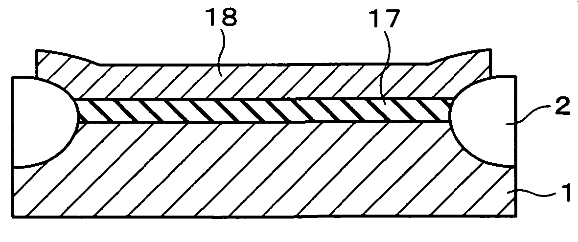
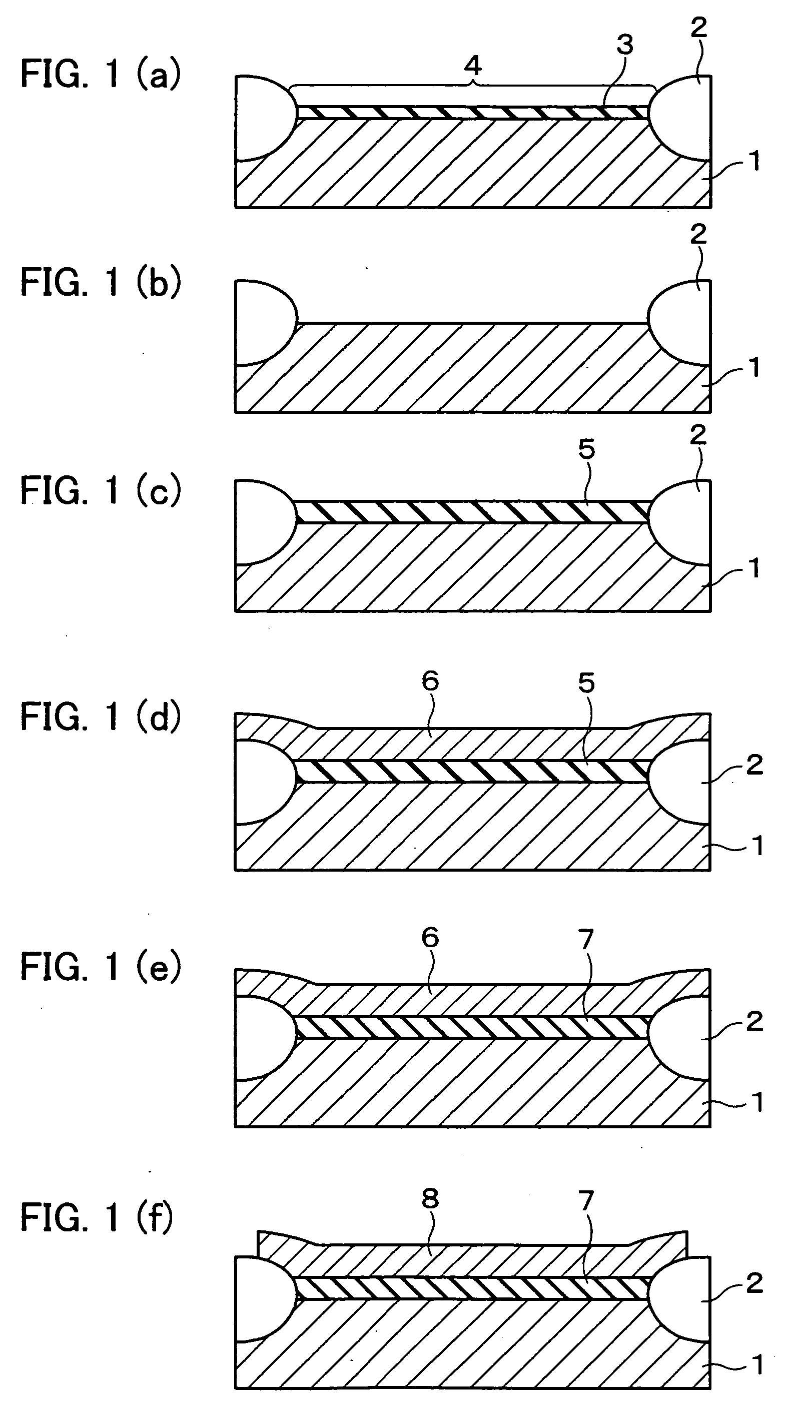
[0080] Described first with reference to FIGS. 1(a) to 1(f) is a method of forming a silicon dioxide film on a silicon substrate in accordance with the present embodiment. In the present embodiment, a step of forming an MOS capacitor by using a silicon substrate is described. Although the present embodiment assumes a case where the silicon dioxide film is formed on a silicon substrate 1, the present invention is also applicable, for example, to a case where the silicon dioxide film is formed on a ball-shaped silicon bulk or on a silicon film formed by epitaxial growth. In this specification, the member (e.g. silicon substrate 1) used as a base of the, silicon dioxide film to be formed is referred to as “silicon substrate”.

[0081] First, an isolation region 2 and an active region 4 were formed on the silicon substrate 1. On a surface of the active region 4, there was a n...

embodiment 2

[0134] The following describes a second embodiment of the present invention, with reference to FIGS. 8(a) to 12.

[0135] Described below with reference to FIGS. 8(a) to 8(e) is a method of forming a silicon dioxide film on a silicon substrate in accordance with the present embodiment. In the present embodiment, the chemical oxide film 5 is formed on the silicon substrate 1 by the steps of FIGS. 8(a) to 8(c), which are respectively identical to FIGS. 1(a) to 1(c) of EMBODIMENT 1. The description on the FIGS. 1(a) to 1(c) of EMBODIMENT 1 is also applicable to the steps of FIGS. 8(a) to 8(c) of the present embodiment.

[0136] After the chemical oxide film 5 was formed, in the present embodiment, the metal film 6 was not formed, but the wafer was heated in a hydrogen-containing gas in an electric furnace. In the present embodiment, the wafer was heated in a mixed gas of hydrogen and nitrogen (nitrogen containing 5% of hydrogen) at 450° C. for 20 minutes.

[0137] This heat processing is per...

embodiment 3

[0160] The following describes a third embodiment of the present invention, with reference to FIG. 14.

[0161] In order to manufacture a flexible liquid crystal display, which has been under development recently, it is necessary to form TFTs on a substrate made of organic substance such as PET. For this purpose, the TFTs must be formed at a low temperature of not higher than 200° C.

[0162] In the case of such TFTs, in general, a relatively high voltage is applied to the gate electrode. Therefore, a silicon dioxide film used as the gate oxide film of the TFTs must have a sufficient thickness so as to avoid dielectric breakdown.

[0163] Conventionally, the silicon dioxide film used as the gate insulating film of the TFTs has been formed through deposition by CVD. However, in order to deposit the silicon dioxide film by CVD, the substrate must be heated to a high temperature of 400° C. to 500° C. Therefore, depositing the silicon dioxide film by CVD is not suitable for forming the TFTs i...


PUM

PropertyMeasurementUnit
temperatureaaaaaaaaaa

Abstract

After cleaning a surface of a silicon substrate (1), impurities and natural oxide film existing on the silicon substrate (1) are removed by soaking the silicon substrate (1) in a 0.5%-by-volume HF aqueous solution for 5 minutes. The silicon substrate (1) is rinsed (cleaned) with ultrapure water for five minutes. Then, the silicon substrate (1) is soaked for 30 minutes in azeotropic nitric acid heated to an azeotropic temperature of 120.7° C. In this way, an extremely thin chemical oxide film (5) is formed on the surface of the silicon substrate (1). Subsequently, a metal film (6) (aluminum-silicon alloy film) is deposited, followed by heating in a hydrogen-containing gas at 200° C. for 20 minutes. Through the heat processing in the hydrogen-containing gas, hydrogen reacts with interface states and defect states in the chemical oxide film (5), causing disappearance of the interface states and defect states. As a result, the quality of the film can be improved. Thus, it is possible to form a high quality (with low leak current density), extremely thin silicon dioxide film on the silicon substrate at a low temperature with excellent film-thickness controllability.

Description

TECHNICAL FIELD [0001] In general, the present invention relates to a method of forming a silicon dioxide film on a surface of a silicon substrate, a method of forming an oxide film on a surface of a semiconductor substrate, and a method of manufacturing a semiconductor device by these methods. These methods can be employed to form an oxide film of an MOS (metal-oxide-semiconductor) device used for semiconductor integrated circuits, especially to form an extremely thin gate oxide film, a capacitor oxide film, and the like of an MOS transistor, an MOS capacitor, and the like. In particular, the present invention relates to a method of forming a high-quality (with little leak current), extremely thin silicon dioxide film and the like with excellent film-thickness controllability. [0002] The present invention also relates to a method of forming, for example, a silicon dioxide film of a TFT (thin-film transistor) at a low temperature. BACKGROUND ART [0003] Recently, the performance of s...

Claims


Application Information

Patent Timeline
Patent Type & Authority Applications(United States)
IPC IPC(8): H01L27/04H01L21/28H01L21/316H01L21/336H01L21/822H01L29/51H01L29/78H01L29/786
CPCH01L21/02238H01L21/02255H01L21/02337H01L29/518H01L21/28202H01L21/31662H01L29/511H01L21/28194H01L21/02164
Inventor KOBAYASHI, HIKARU
Owner JAPAN SCI & TECH CORP
Why Eureka
Try Eureka