Wafer supporting member

a supporting member and wafer technology, applied in the direction of hot plate heating arrangements, transportation and packaging, passenger space, etc., can solve the problems of affecting the wafer, exhibiting a bad cooling efficiency, and conductive base parts having a part of the adsorption force remaining, so as to reduce temperature unbalance, reduce the time to transfer heat, and increase the throughput at the machining process

Inactive Publication Date: 2005-09-29
KYOCERA CORP
View PDF9 Cites 103 Cited by
  • Summary
  • Abstract
  • Description
  • Claims
  • Application Information

AI Technical Summary

Benefits of technology

[0032] In addition, by defining a minimum thickness of the resin filled in the concave portion provided on the surface of the heater in a range of 0.01 to 1 μm, the wafer supporting member can noticeably reduce temperature unbalance on the mounting surface while reducing time to transfer heat on the mounting surface of the planar body, and increase throughput at machining process.
[0033] In manufacturing the wafer supporting member, the adhesive layer is preferably formed laminating alternative resin layers thinner than the adhesive layer between the heater part and the conductive base part several times, for exampler by laminating an adhesive layer between the heater part and the conductive base part multiple times by means of a screen ...

Problems solved by technology

Such insulating sheet has problems in heat-resistance, abrasion-resistance, chemical-resistance and so forth, as well as in cleanness since it has small hardness to cause generation of ground powders in use easy to stick on the semiconductor wafer, thereby adversely affecting the wafer.
But this has disadvantages in that it composed of alumina having a low thermal conductivity and the insulating sheet 22 is porous, thereby exhibiting a bad cooling efficiency.
However, the wafer supporting member according to Japanese Unexamined Patent Application Publication No. 4-287344 has defects in that the conductive base part has part of the adsorption force remained, since a residual charge on the mounting surface remains on the insulating adsorption layer and has troubles to flow into the conductive base part, whereby the wafer W cannot be separated in a short time.
However, a protective film with about 10 μm thickness is difficult to fill pinholes generated during a film for...

Method used


Image

  • Wafer supporting member
  • Wafer supporting member
  • Wafer supporting member

Examples


first embodiment

[0051] Hereinafter, a first embodiment (an electrostatic chuck) of the present invention will be described in details below.

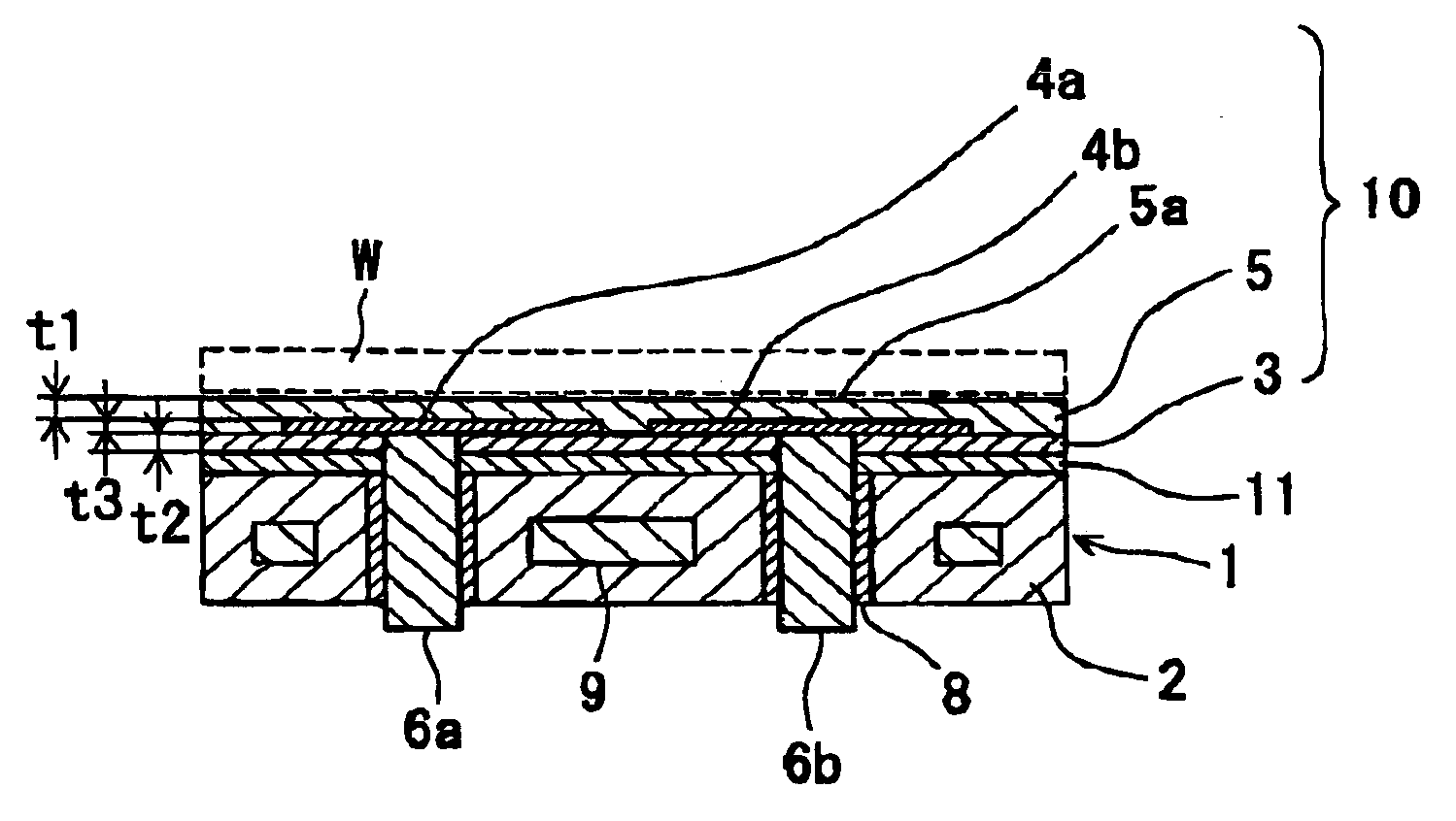
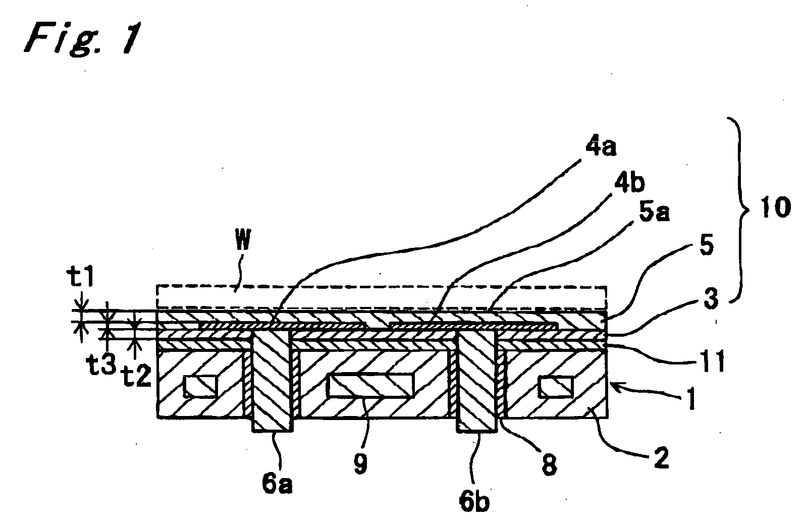
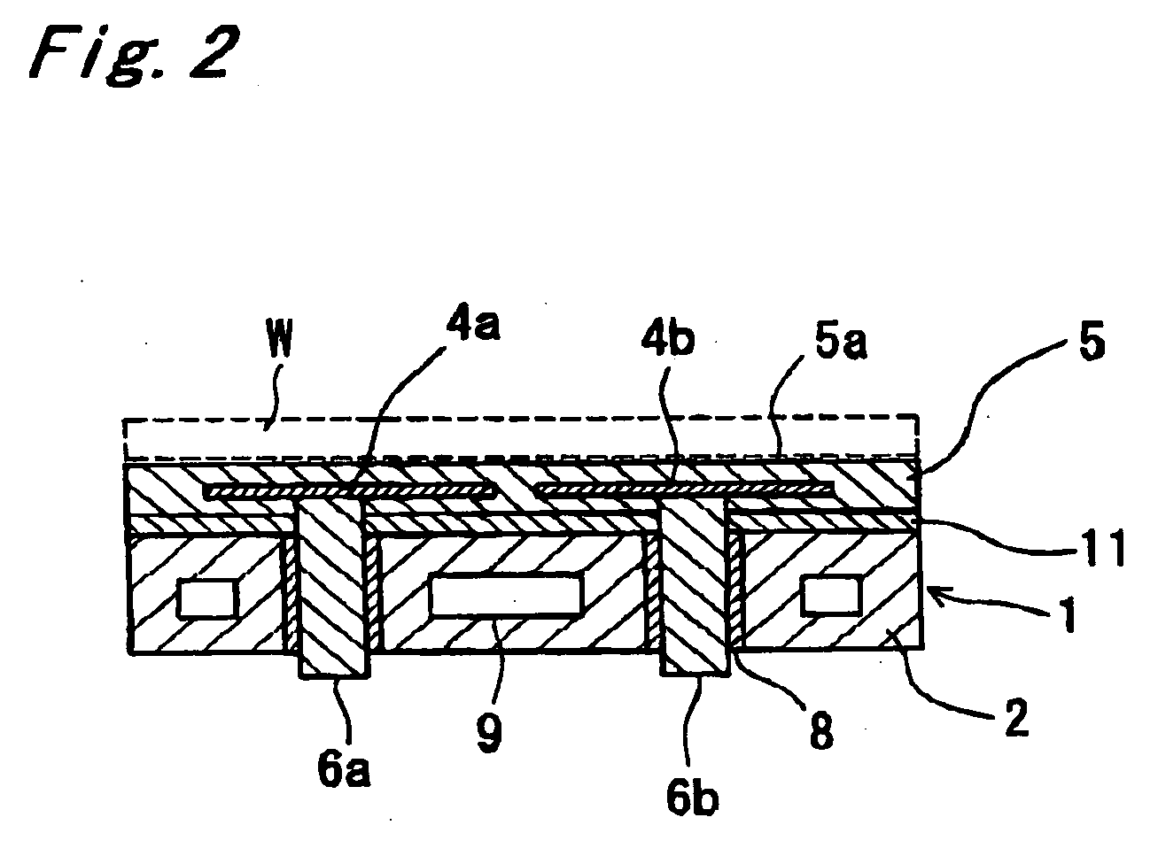
[0052] In the first embodiment of the present invention, the wafer supporting member includes an supporting part including a main surface as a mounting surface for mounting a wafer and the other main surface having an insulating layer provided with a built-in adsorption electrode and having an insulating sheet; the insulating resin layer optionally having a heater attached to the main surface having the adsorption election built therein; and a conductive base part with a passage through which cooling medium flows in, and the resin layer of the wafer supporting member has a volume resistivity in a range of 108 to 1014 Ω·cm. Also, the resistance value between the mounting surface and the conductive base part is preferably in a range of 107 to 1013 Ω. Both of the insulating sheet and the insulating layer are formed of the same planar ceramic body, in which the ab...

example 1

[0129] To the alumina powders, 0.5% by mass of calcium oxide and magnesium oxide in terms of weight were added, which was then mixed using a ball-mill for 48 hours. The obtained alumina slurry passed through a sieve of 325 meshes to remove the impurities attached on the ball or the ball-mill wall, and then dried in a dryer at 120° C. for 24 hours. To the obtained alumina powders, an acrylic binder and a solvent were added and mixed to prepare an alumina slurry. Using this alumina slurry, a green tape was prepared by a doctor blade method.

[0130] Further, several sheets of the green tape were laminated to form a laminate and, on one main surface thereof, an adsorption electrode made of a tungsten carbide paste was printed. On the other hand, several sheets of the separate ceramic green sheets were laminated to form a laminate, which was compressed under pressure to obtain a compressed laminate.

[0131] In addition, the laminate was baked in a baking furnace comprising a W heater and a...

example 2

[0148] In the similar way to that of Example 1, a wafer supporting member made of alumina and aluminum nitride was prepared. The aluminum nitride used had various volume resistivities of the materials by varying the amount of the added cerium oxide within a range or 1 to 15% by mass. The samples were prepared, having different volume resistivities by varying the content of Al in the resin layer. In the same manners as in Example 1, the samples were evaluated. Then, the electric resistance value between the mounting surface and the conductive base part was determined for each of the samples.

[0149] For the electric resistance value between the mounting surface and the conductive base part, an electrode with a diameter of 10 mm was installed on the mounting surface, and the electric resistance value between the electrode and the conductive base part. The measured electric resistance value was taken as a resistance value between the mounting surface and the conductive substrate as calc...


PUM


Abstract

The present wafer supporting member includes a supporting part composed of a planar insulating sheet having a pair of main surfaces, one serving as a mounting surface for mounting a wafer and the other having an adsorption electrode; a resin layer part provided below the adsorption part and a conductive base part provided below the resin layer part wherein the adsorption part has a thickness in a range of 0.02 to 10.5 mm, preferably 0.02 to 2.0 mm. The wafer supporting member further comprises a heater part provided with an insulating resin layer having heaters embedded therein between the resin layer part and the conductive base part. On a surface of the insulating resin layer concave portions are formed and filled with a resin having a composition different from that of the insulating resin layer in order to embed the concave portions.

Description

BACKGROUND OF THE INVENTION [0001] 1. Field of the Invention [0002] The present invention relates to a supporting member for holding a wafer or a liquid crystal glass (hereinafter collectively referred to as a ‘wafer supporting member’), which is used in a method of manufacturing a semiconductor or liquid crystal, including etching for microfabrication of a semiconductor water and / or a liquid crystal glass, forming a thin film, exposing a photoresist film, etc. [0003] 2. Description of the Related Art [0004] Conventional manufacturing of a semiconductor includes etching for micro-fabrication of a wafer, forming a thin film, exposing a photoresist film, etc., which uses a wafer supporting member for electrostatically adsorbing the wafer in order to hold it. [0005] The wafer supporting member, as shown in FIG. 7, includes a ceramic substrate 54, a pair of adsorption electrodes 53 provided on the upper surface of the ceramic substrate, feeding terminals 58 for energizing the adsorption...

Claims


Application Information

Patent Timeline
IPC IPC(8): H01L21/00H05B3/20H01L21/02H01L21/205H01L21/3065H01L21/31H01L21/68H01L21/683H05B3/74
CPCH01L21/67103H01L21/6831H01L21/67109B42D5/065B42D1/006B60R7/08B60R2011/0003
Inventor NAKAMURA, TSUNEHIKOMIGITA, YASUSHIMATSUOKA, TOHRU
Owner KYOCERA CORP
Why Eureka
Try Eureka