Integrated circuit device

a circuit device and integrated circuit technology, applied in the direction of instruments, basic electric elements, heat measurement, etc., can solve the problems of insufficient signal-to-noise ratio (signal-to-noise ratio), inability to acquire sufficient snr (signal-to-noise ratio), and inability to achieve uniform ambient temperature of resistors, etc., to achieve accurate measurement, enhance the uniform heat providing effect, and improve the thermal conduction of the thermal conducting layer

Active Publication Date: 2005-10-06
RENESAS ELECTRONICS CORP
View PDF1 Cites 19 Cited by
  • Summary
  • Abstract
  • Description
  • Claims
  • Application Information

AI Technical Summary

Benefits of technology

[0014] Further, it is preferable that the thermal conducting layer should be formed of one metal selected from a group of aluminum, copper and titanium, or an alloy of the metal, or an alloy essentially consisting of two or more metals in the group. This improves the thermal conduction of the thermal conducting layer, thereby further enhancing the uniform heat providing effect.
[0015] It is further preferable that the temperature monitor element should be formed of vanadium oxide. This makes it possible to acquire the temperature monitor element the temperature coefficient of whose electric resistivity has a large absolute value, so that the temperature can be measured accurately.
[0016] It is preferable that the thermal conducting layer should be connected to the temperature monitor element. This can permit heat accumulated in the thermal conducting layer to be promptly discharged via the thermal conducting layer, thereby improving the response to temperature measurement.
[0017] It is also preferable that the integrated circuit device should further comprise a substrate on which the temperature monitor element and the thermal conducting layer should be provided and to which the thermal conducting layer is connected. This can allow heat accumulated in the thermal conducting layer to promptly escape to the substrate, thereby improving the response to temperature measurement.
[0018] Furthermore, it is preferable that the integrated circuit device should further comprise: a substrate; a multi-layer wiring structure which is provided on the substrate and on which the temperature monitor element and the thermal conducting layer are provided; and a logic circuit section provided at a top surface of the substrate and wiring layers located below a topmost layer of the multi-layer wiring structure, the temperature monitor element being provided at the topmost layer of the multi-layer wiring structure. This can prevent the logic circuit section from being contaminated by the material for the temperature monitor element.
[0019] According to the present invention, as the thermal conducting layer is provided at least either above or under the temperature monitor element, the ambient temperature of the temperature monitor element can be made uniform, so that the temperature can be measured accurately and stably.

Problems solved by technology

The technique that uses a parasitic pn diode as a temperature sensor has a problem such that as the temperature coefficient of the parasitic pn junction diode is as low as 0.2 (% / K), therefore a sufficient SNR (Signal-to-Noise Ratio) cannot be acquired.
The prior art technique suffers the following problems.
When a resistor consisting of a vanadium oxide, for example, is formed and the temperature of an integrated circuit device is measured by measuring the resistance of the resistor, the ambient temperature of the resistor may not become uniform due to the influence of the internal and external environments of the integrated circuit device.
For example, the flow of the current to wires or the like provided around the resistor locally raises the temperature, thus making the ambient temperature non-uniform.
In this case, the internal temperature of the resistor becomes non-uniform, thus making the internal resistivity of the resistor non-uniform, so that the temperature cannot be measured accurately or stably.

Method used


Image

  • Integrated circuit device
  • Integrated circuit device
  • Integrated circuit device

Examples


Embodiment Construction

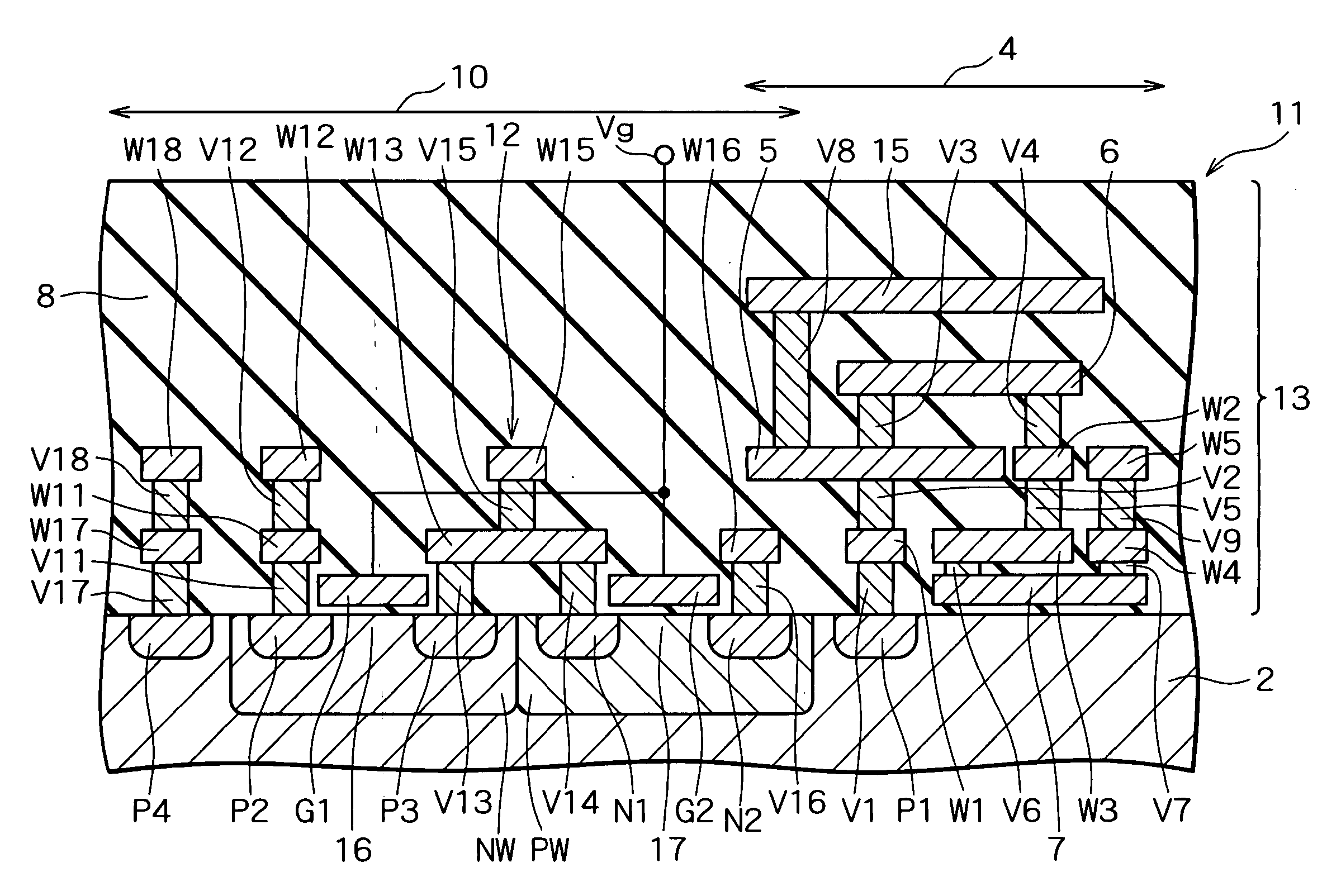
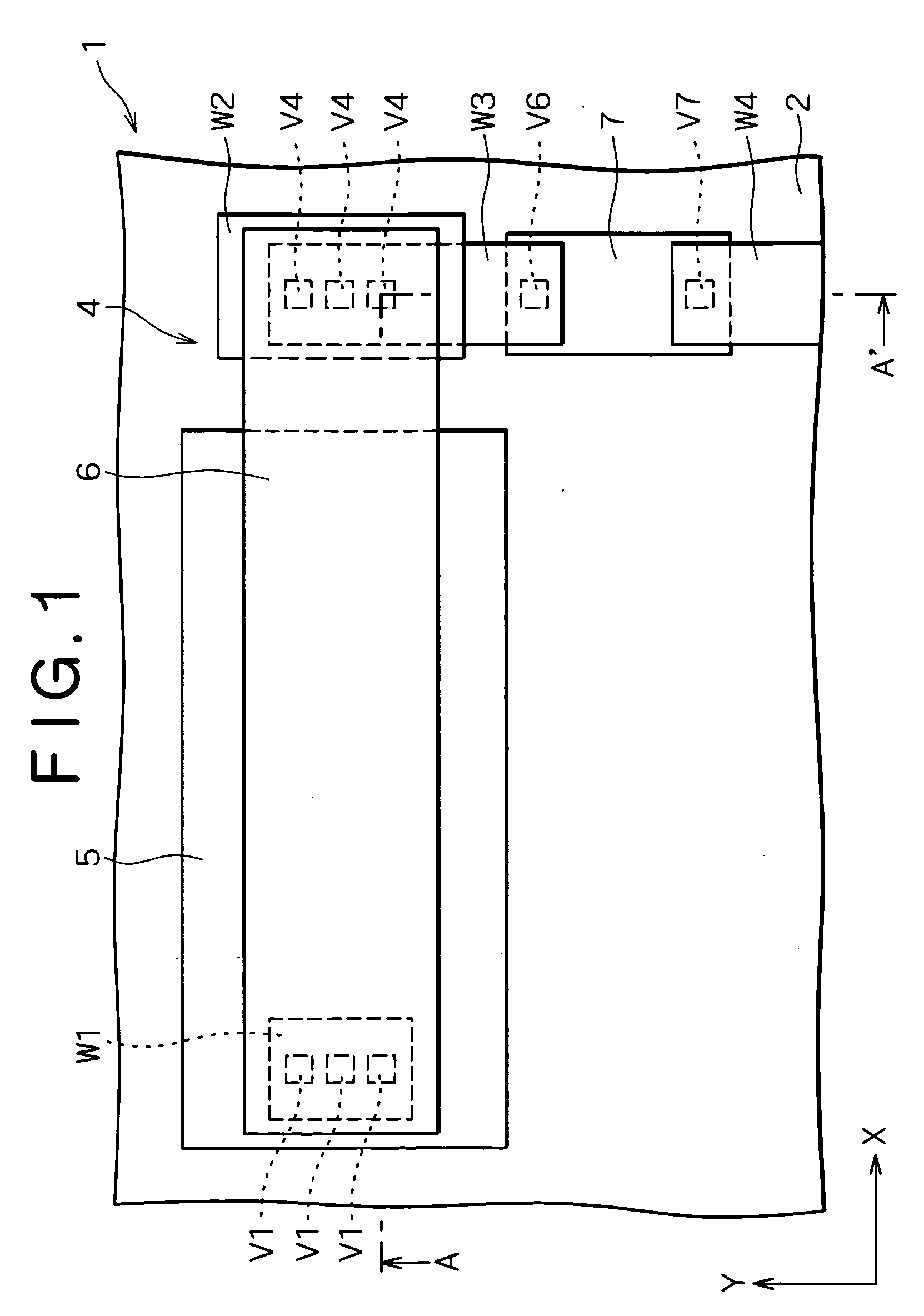
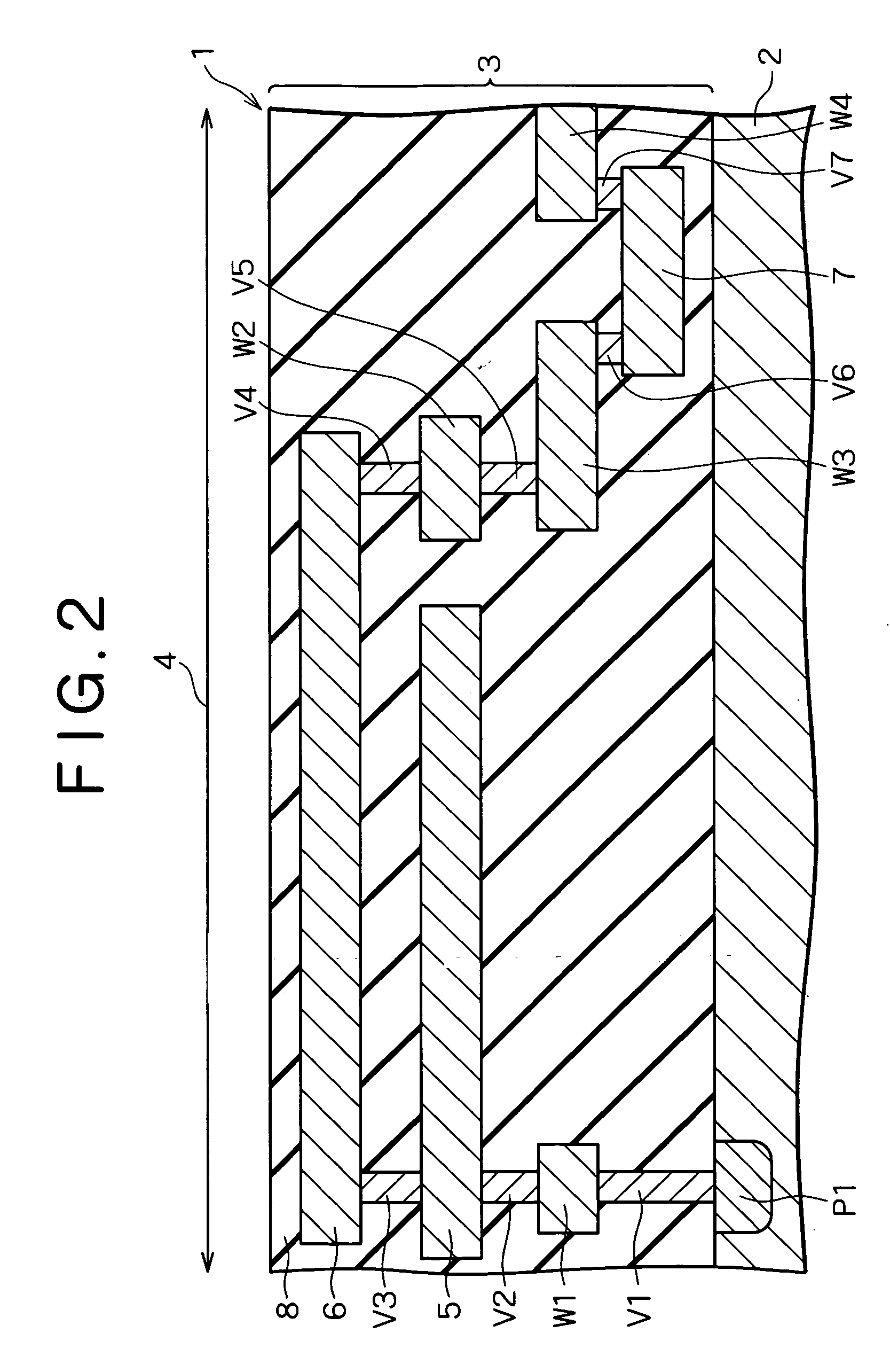
[0025] Preferred embodiments of the invention will be described specifically below with reference to the accompanying drawings. To begin with, the first embodiment of the invention will be discussed. FIG. 1 is a plan view showing a semiconductor integrated circuit device according to the first embodiment of the invention, FIG. 2 is a cross-sectional view along line A-A′ shown in FIG. 1, and FIG. 3 is an equivalent circuit diagram showing a temperature sensor section of the semiconductor integrated circuit device shown in FIGS. 1 and 2. The semiconductor integrated circuit device according to the embodiment is formed on a single silicon chip.

[0026] As shown in FIGS. 1 and 2, the semiconductor integrated circuit device 1 according to the embodiment is provided with a silicon substrate 2 of, for example, P type on which a multi-layer wiring structure 3 is provided. The multi-layer wiring layer 3 includes plural wiring layers and plural insulating layers alternately laminated. For exam...


PUM

PropertyMeasurementUnit
thicknessaaaaaaaaaa
lengthaaaaaaaaaa
lengthaaaaaaaaaa

Abstract

In a semiconductor integrated circuit device, a sheet-like temperature monitor member of vanadium oxide is provided, whose one end is connected to one via while the other end is connected to another via. A sheet-like thermal conducting layer of aluminum is provided below the temperature monitor member. A region equal to or greater than a half of the entire temperature monitor member overlies the thermal conducting layer in a plan view.

Description

BACKGROUND OF THE INVENTION [0001] 1. Field of the Invention [0002] The present invention relates to an integrated circuit device with a built-in monolithic temperature sensor. [0003] 2. Description of the Related Art [0004] Recently, there are growing needs for monitoring the operation temperature of an integrated circuit device for the purpose of preventing thermal breakdown of devices in the integrated circuit device and stabilizing the operation of a device whose characteristic has temperature dependence. [0005] In this respect, Japanese Patent Laid-Open Publication No. H1-302849, for example, discloses a technique of providing a temperature sensor on the same substrate as that of an LSI (Large Scale Integrated circuit). In the technique, the temperature sensor decides that the LSI is abnormally overheated when the temperature detected by the temperature sensor exceeds a predetermined value and then shutting down the LSI. Therefore, it can protect the LSI from thermally broken b...

Claims


Application Information

Patent Timeline
Patent Type & Authority Applications(United States)
IPC IPC(8): H01L23/52G01K7/16H01L21/3205H01L21/822H01L23/34H01L23/522H01L23/58H01L27/00H01L27/04H01L31/058
CPCG01K7/16H01L23/34H01L23/522H01L2924/0002H01L2924/00
Inventor OHKUBO, HIROAKINAKASHIBA, YASUTAKAKAWAHARA, NAOYOSHIMURASE, HIROSHIODA, NAOKISASAKI, TOKUHITOITO, NOBUKAZU
Owner RENESAS ELECTRONICS CORP
Why Eureka
Try Eureka