Semiconductor device, method of manufacturing the same, and electronic device

a technology of semiconductor devices and resistive elements, which is applied in the direction of solid-state devices, pulse generators, pulse techniques, etc., can solve the problems of low accuracy of resistance control, affecting the operation of the device, etc., to achieve high sheet resistance, good operational characteristics, and high accuracy

Inactive Publication Date: 2005-10-06
RICOH KK
View PDF6 Cites 11 Cited by
  • Summary
  • Abstract
  • Description
  • Claims
  • Application Information

AI Technical Summary

Benefits of technology

[0048] According to the above-described method, it is possible to control the resistance and the temperature coefficient of a resistive element with high accuracy.
[0049] According to the present invention, a resistor having a positive temperature coefficient and high sheet resistance is employed for a resistive element of the semiconductor device. Accordingly, it is possible to control variations in the resistance and the temperature coefficient of the resistive element, and thus to provide a semiconductor device having good operational characteristics.

Problems solved by technology

The first problem is that the accuracy of the resistance control is low so that the obtained resistance varies greatly.
The second problem is that it is difficult to accurately control the rate of change in the resistance of the resistive element with respect to a change in temperature, that is, it is difficult to control the temperature coefficient of the resistive element with accuracy.
The third problem is that the control of the resistance can be performed only in a direction to increase the resistance and it is difficult to correct the control once it has been performed because the resistance is controlled by cutting off interconnection lines.
However, in the case of using the correction device illustrated in FIG. 1, there is a problem in that the configuration of the correction device is complicated so as to increase a circuit in scale.
In this case, however, it is difficult in particular to employ a resistor having a positive temperature coefficient for the following reasons, which causes a problem in that it is difficult to achieve a desired temperature coefficient.
For instance, in the case of using the conventionally used resistor using a Si impurity diffusion layer or formed of polysilicon, it is difficult to increase sheet resistance.
Therefore, an attempt to obtain a desired resistance in a circuit to be formed increases the resistor size.
This makes it difficult to use such a resistor in a normal-size circuit, and also causes a problem in that it is difficult to miniaturize the circuit.
Further, in the case of employing a resistive element using a resistor having a positive temperature coefficient and the conventionally used resistor having a negative temperature coefficient in combination, an attempt to control the temperature coefficient of the resistive element by combining the resistors may result in a problem because the resistors differ greatly in sheet resistance.
For instance, since the resistor having the positive temperature coefficient and the resistor having the negative temperature coefficient differ greatly in size in the circuit, there is a difference in processing accuracy between the resistors in the process of forming the resistors, such as an etching process, and the processing process is also complicated.
In some cases, this makes it difficult to control the resistance and the temperature coefficient of each resistor with accuracy.
Further, for instance, with a resistor using an N-type well layer, it is possible to form a resistor having a positive temperature coefficient and a high sheet resistance, but it is difficult to form a resistor having a small line width.
As a result, the area occupied by the resistor increases, which, in some cases, makes it difficult to miniaturize a circuit using the resistor.
However, there is a problem in that a method and technique for such accurate measurement have not been established completely.
For instance, if a test terminal is provided directly to a resistor in the oscillation circuit in order to measure the temperature characteristic of the resistor, the circuit cannot be expected to operate with accuracy because of the parasitic capacitance of the terminal and noise.
However, it is difficult to equalize measurement conditions such as the sheet number and the bias voltage of the monitoring means with those in its operating state in which the monitoring means is incorporated into the actual circuit.
Further, there is another possible problem in the conventional resistor control method.
For instance, it may be difficult to control a resistor in the oscillation circuit illustrated in FIG. 2 or the amplifier circuit illustrated in FIG. 3 only by previously providing multiple interconnection lines that short-circuit the resistors forming a resistive element, and cutting off one or more of the interconnection lines in accordance with the results of circuit measurement.
Accordingly, it is difficult to determine the degree of change by changing the resistance in both increasing and decreasing directions at the stage of controlling the resistive element.
In the case of, for instance, the oscillation circuit illustrated in FIG. 2, this causes a problem in that if a frequency before the control is offset from a target frequency, the operational delays of the comparator 21 and the inverters 25 and 26 have effects different from those on the controlled frequency, so that an accurate frequency correction cannot be obtained.
Further, there is also a possibility in the amplifier circuit illustrated in FIG. 3 that if the resistance differs greatly between before and after controlling, a change is caused in the characteristic because of the effect of noise, so that a desired characteristic cannot be obtained.
That is, in these circuits, it is difficult to accurately measure the resistance and the temperature coefficient of a resistor in a state close to the actual form of usage, thus causing a problem in that it is difficult to obtain a desired characteristic by controlling the resistance and the temperature coefficient of the resistor with accuracy.

Method used


Image

  • Semiconductor device, method of manufacturing the same, and electronic device
  • Semiconductor device, method of manufacturing the same, and electronic device
  • Semiconductor device, method of manufacturing the same, and electronic device

Examples


first embodiment

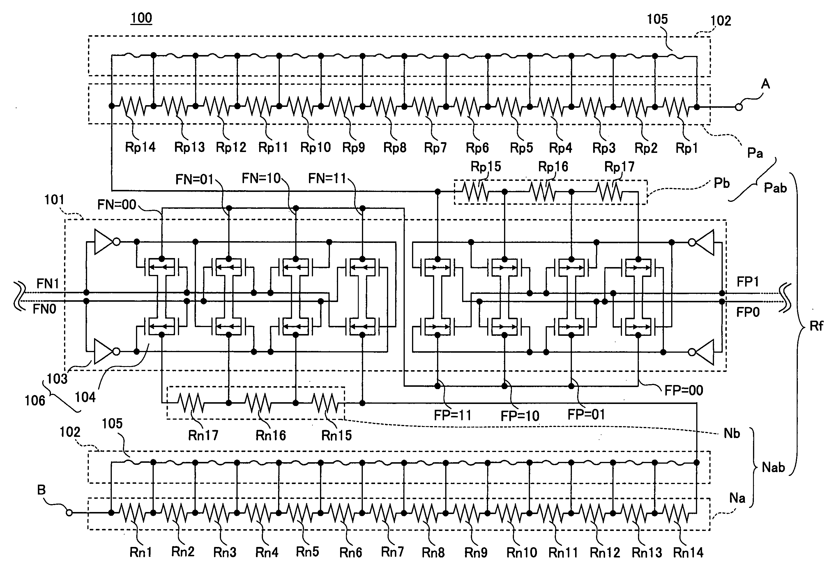
[0066]FIG. 4 is a schematic diagram illustrating a semiconductor device 100 including a resistive element according to a first embodiment of the present invention.

[0067] Referring to FIG. 4, the semiconductor device 100 includes a resistive element Rf formed between a terminal A and a terminal B. The resistive element Rf includes resistive elements having different temperature coefficients, that is, a resistive element Pab having a positive temperature coefficient and a resistive element Nab having a negative temperature coefficient. The resistive elements Pab and Nab are connected in series, for instance.

[0068] The resistive element Pab includes multiple resistors of a positive temperature coefficient connected in series. The resistive element Nab includes multiple resistors of a negative temperature coefficient connected in series. The semiconductor device 100 includes a connection change part that changes the state of connection of these resistors. It is possible to control the...

second embodiment

[0113] The semiconductor device 100 may also be configured as follows. FIG. 6 is a schematic diagram illustrating a variation (configuration) of the semiconductor device 100 according to a second embodiment of the present invention. In FIG. 6, the same elements as those described above are referred to by the same numerals, and a description thereof is omitted.

[0114] Referring to FIG. 6, the semiconductor device 100 includes a detection part 111. The detection part 111 detects a change in the environment of the semiconductor device 100, such as a change in temperature. Employment of the detection part 111 makes it possible to provide the semiconductor device 100 with good characteristics irrespective of environmental changes.

[0115] The connection change part 101 may select the sheet number of the positive functioning resistors (the number of resistors of the positive temperature coefficient that function, that is, substantially get connected, in the resistive element Rf) and the sh...

third embodiment

[0121] The semiconductor device 100 may be applied to a wide variety of electronic devices. FIG. 7 is a circuit diagram illustrating an electronic device 150 in which the semiconductor device 100 is applied to a CR oscillation circuit according to a third embodiment of the present invention. InFIG. 7, the same elements as those described above are referred to by the same numerals, and a description thereof is omitted.

[0122] In the case of FIG. 7, the number of resistors of the semiconductor device 100 is changed from that in the case of FIG. 4. Thus, the number of resistors and the sheet number of resistors are changed as desired when employed in the semiconductor device 100. The same holds true for the following embodiments.

[0123] Referring to FIG. 7, the electronic device 150 having an oscillation circuit includes a comparator 121, a reference voltage generator circuit 120, a capacitor 130, the semiconductor device 100, and inverters 122, 123, and 124. The capacitor 130 and the ...


PUM


Abstract

A semiconductor device is disclosed that includes a resistive element including a first resistor having a positive temperature coefficient and a second resistor having a negative temperature coefficient. The first resistor includes a metal film.

Description

BACKGROUND OF THE INVENTION [0001] 1. Field of the Invention [0002] The present invention relates generally to semiconductor devices, methods of manufacturing the same, and electronic devices, and more particularly to a semiconductor device including a resistive element, a method of manufacturing the same, and an electronic device employing the same. [0003] 2. Description of the Related Art [0004] Conventionally, resistors such as those using a Si impurity diffusion layer and those formed of polysilicon have been widely used for forming a resistive element incorporated into semiconductor devices and electronic devices. The resistance of such a resistive element is controlled by, for instance, previously providing multiple interconnection lines that short-circuit the resistors forming the resistive element, and cutting off one or more of the interconnection lines in accordance with the results of circuit measurement. In this case, in part of the resistive element where the interconne...

Claims


Application Information

Patent Timeline
Patent Type & Authority Applications(United States)
IPC IPC(8): H01L27/04H01C7/06H01L21/82H01L21/822H01L27/08H03K3/0231H03K3/354
CPCH03K3/0231H01L27/0802
Inventor YOSHIKAWA, REI
Owner RICOH KK
Why Eureka
Try Eureka