Semiconductor integrated circuit
a technology of integrated circuits and semiconductors, applied in semiconductor devices, digital storage, instruments, etc., can solve problems such as deterioration of signal margins, and achieve the effects of reducing channel current needed for program execution, reducing storage charge for detection, and increasing programming efficiency
- Summary
- Abstract
- Description
- Claims
- Application Information
AI Technical Summary
Benefits of technology
Problems solved by technology
Method used
Image

Examples
first embodiment
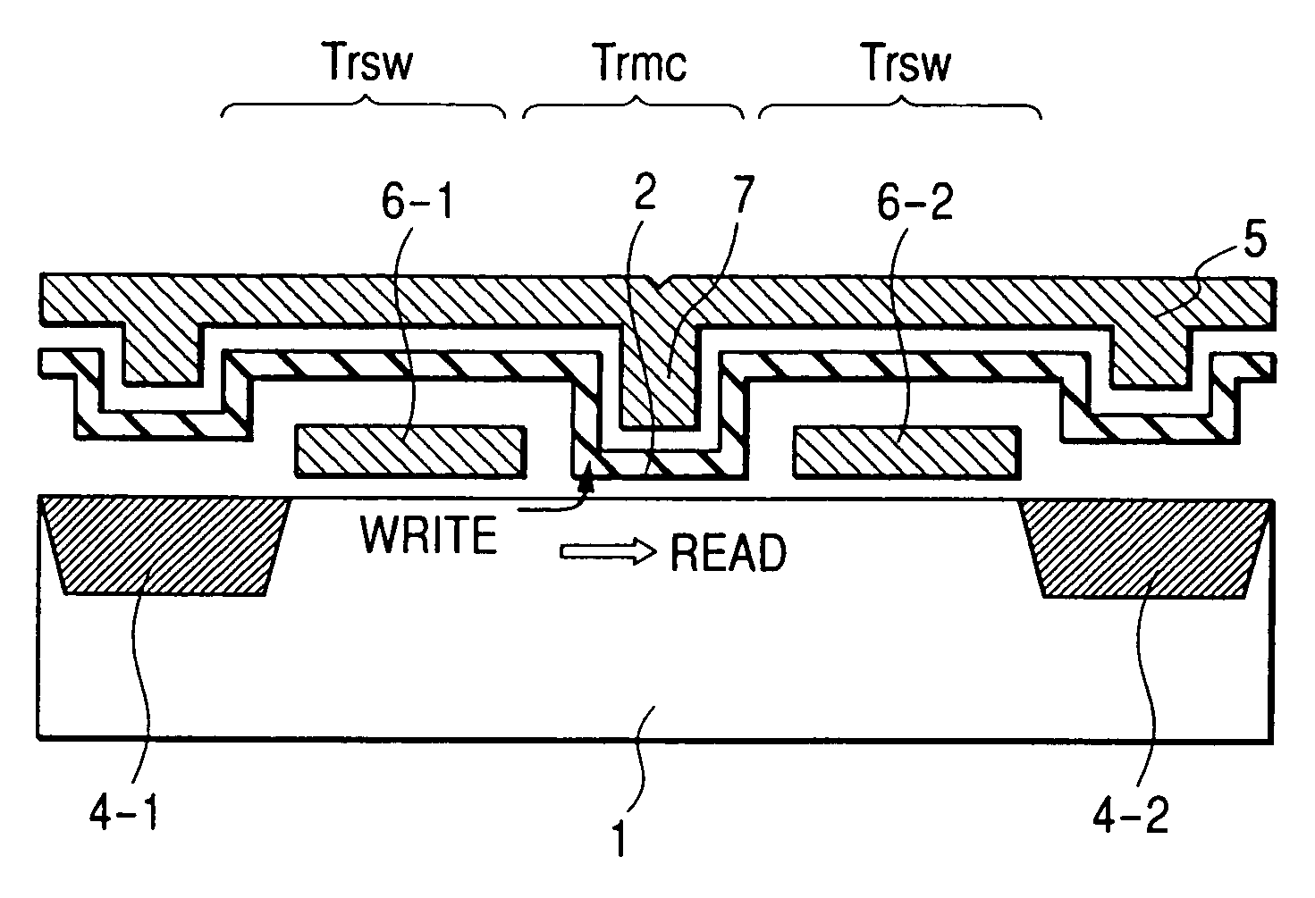
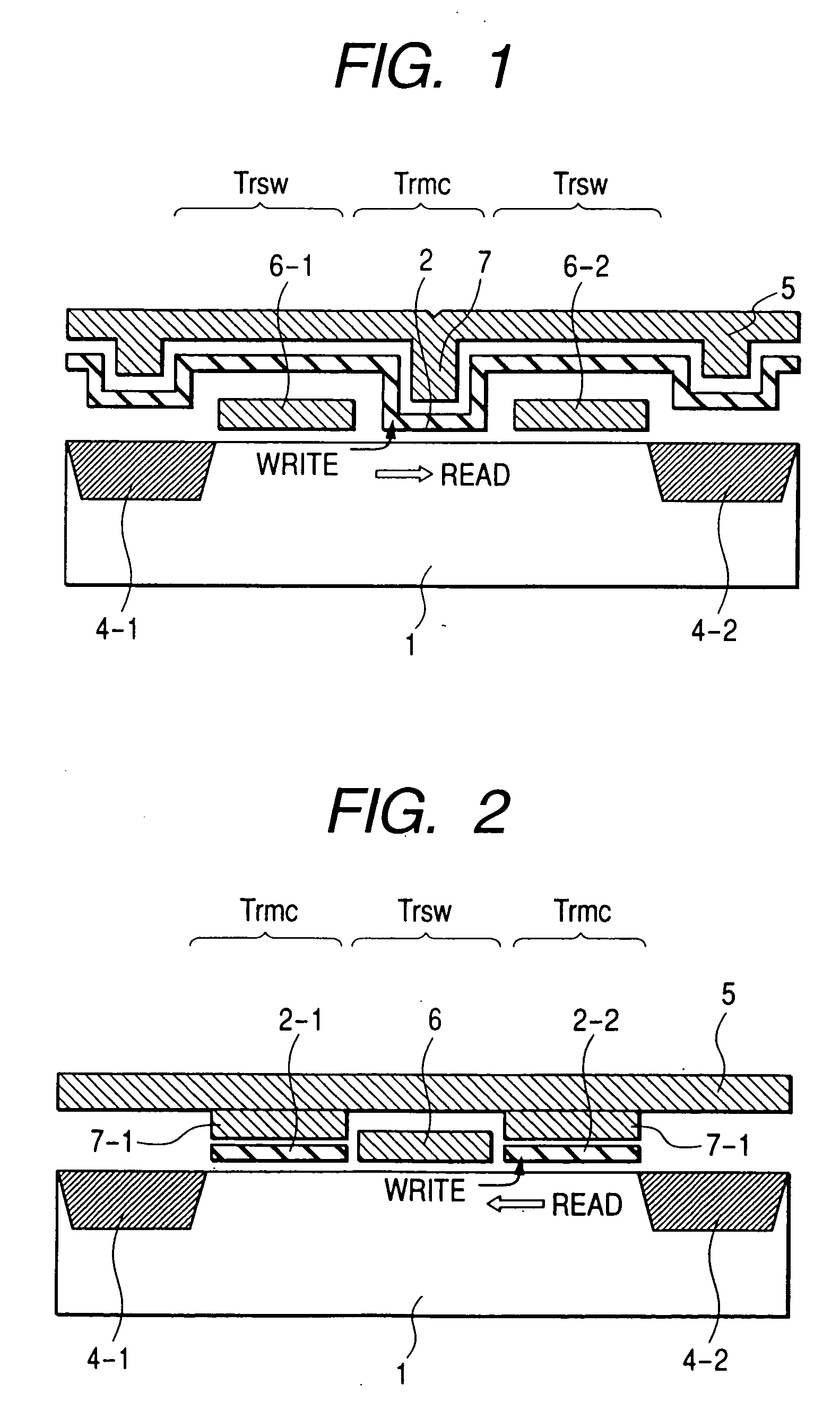
[0140] A memory cell structure, in which switch transistors Trsw are disposed on both the sides of a memory transistor Memory transistor Trmc, is employed as a multi-storage nonvolatile memory cell in order to solve the problems of an increase in programming speed in program, read disturb during read, and an expansion of a dual-way signal read margin. While a certain amount of reduction of a degree of density cannot help being sacrificed by the provision of the switch transistors Trsw on both the sides of the memory transistor Trmc, FIGS. 14 to 16 exemplify a structure in which a reduction of the degree of density is suppressed utilizing self-aligning diffusion. It should be understood that the term “transistor” used in the specification is an expression conveniently used to make it easy to understand the structure of the multi-storage nonvolatile memory cell according to the present invention and does not mean a perfect transistor, and it is only an expression with an attention pai...
second embodiment
[0144] FIGS. 17 to 20 show a first example of an operation bias when a cell array is made of memory cells provided by the present invention of FIGS. 14 to 16, and FIGS. 21 to 24 show the operation bias. In any of the operation biases, the memory gate electrode 7 of the memory transistor Trmc is connected to word lines 5Li and 5Lj which are shown typically. Bit line / source lines 4Li, 4Lj and 41k, which are typically shown, are disposed so as to intersect the word lines 5Li and 5Lj. Further, switch control lines 6Li to 6Ll, which are typically shown and connected to the switch gate electrodes 6-1, 6-2 of the switch transistors Trsw on both the sides of the memory transistor Trmc, also intersect the word lines 5Li and 5Lj.
[0145]FIG. 17 shows a bias relationship in page mode erase. A relatively large bias of 9 V is applied to only the selected word line 5Lj and a 0 V is applied to all the other word lines. In the erase of a selected memory transistor, trapped electrons are drawn out to ...
third embodiment
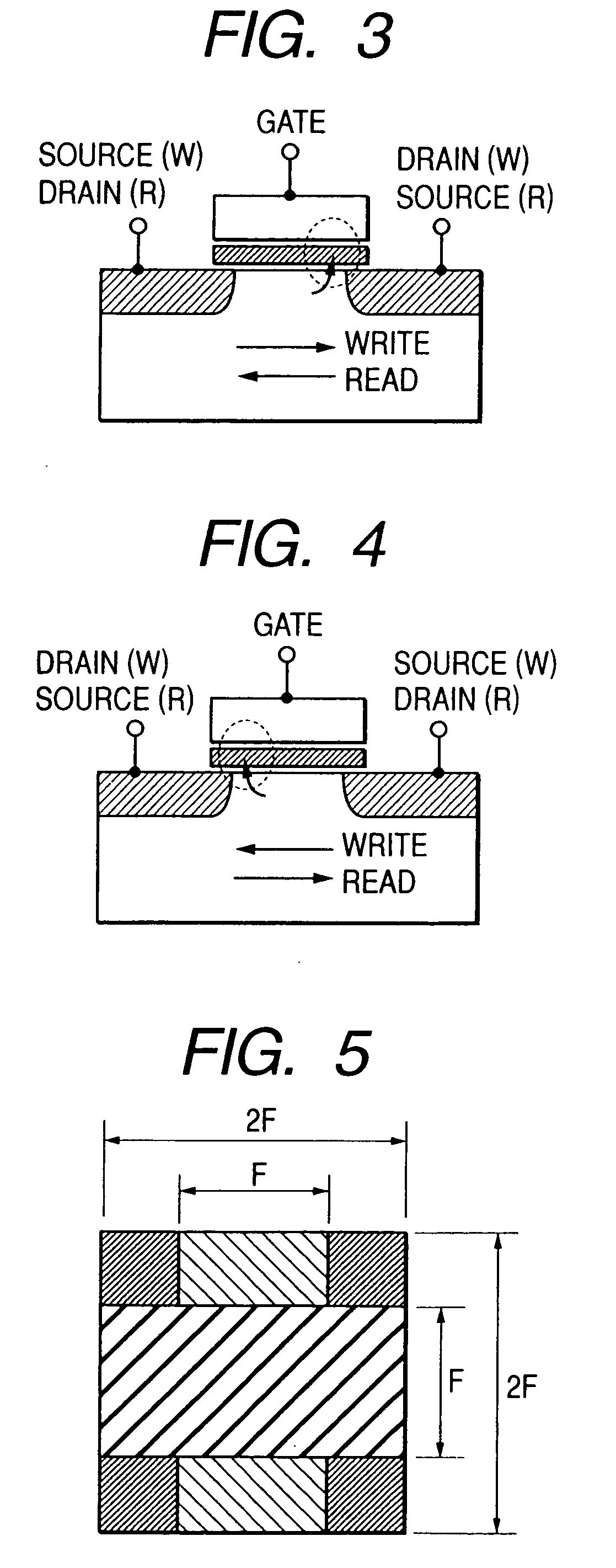
[0183] As exemplified in FIGS. 52 and 53, the memory cell of the third embodiment employs hot-electron source side injection during program and detects a current in the same direction also during read. Since an operation in an opposite direction also is possible in the memory cell, one memory cell can carry out a 2-bit operation. As shown in the layout, one memory cell has a size of 4F2 and its size per 1 bit of data is 2F2, whereby high density can be realized.
[0184] The erase, program and read operations of the memory cell of the third embodiment will be described with reference to FIGS. 54 to 57. In the figures, the switch gate electrodes 6Li, 6Lj and 6Lk of the switch transistors Trsw and the inversion layer lines 20Li, 20Li and 20Lk of the switch transistors Trsw are illustrated as if they are the same lines. Voltages of a semiconductor region constituting the inversion layers are shown in the lower portions of the figures and voltages of the switch gate electrodes are shown in...
PUM
 Abstract
Description
Claims
Application Information
 - R&D
- Intellectual Property
- Life Sciences
- Materials
- Tech Scout
- Unparalleled Data Quality
- Higher Quality Content
- 60% Fewer Hallucinations
Browse by: Latest US Patents, China's latest patents, Technical Efficacy Thesaurus, Application Domain, Technology Topic, Popular Technical Reports.
© 2025 PatSnap. All rights reserved.Legal|Privacy policy|Modern Slavery Act Transparency Statement|Sitemap|About US| Contact US: help@patsnap.com