Method for manufacturing semiconductor device

a manufacturing method and semiconductor technology, applied in semiconductor devices, heat-resistant fibres, textiles and paper, etc., can solve the problems of reducing device performance and reducing breakdown voltag

Active Publication Date: 2005-10-06
SUMCO CORP +1
View PDF19 Cites 97 Cited by
  • Summary
  • Abstract
  • Description
  • Claims
  • Application Information

AI Technical Summary

Benefits of technology

[0010] In the above method, the halogenide gas works as an etching gas, and the etching rate of the halogenide gas is controlled by supply of the gas. Therefore, the etching rate of the epitaxial film at the opening of the trench is higher than that at a position of the trench deeper than the opening of the trench. Thus, the growth rate of the epitaxial film at the opening of the trench is lower than that at a position of the trench deeper than the opening of the trench. Therefore, the epitaxial film is prevented from closing the opening of the trench so that the epitaxial film is filled in the trench without any void. Thus, the above method provides the substrate including the epitaxial film filled in the trench with void-less structure.

Problems solved by technology

In this case, when a defect (i.e., a void) occurs in the epitaxial film filled in the trenches, a breakdown occurs at an upper portion of the void, which results in reducing a breakdown voltage.
In this manner, the influence of defects in the filled epitaxial film reduces the performance of a device.

Method used

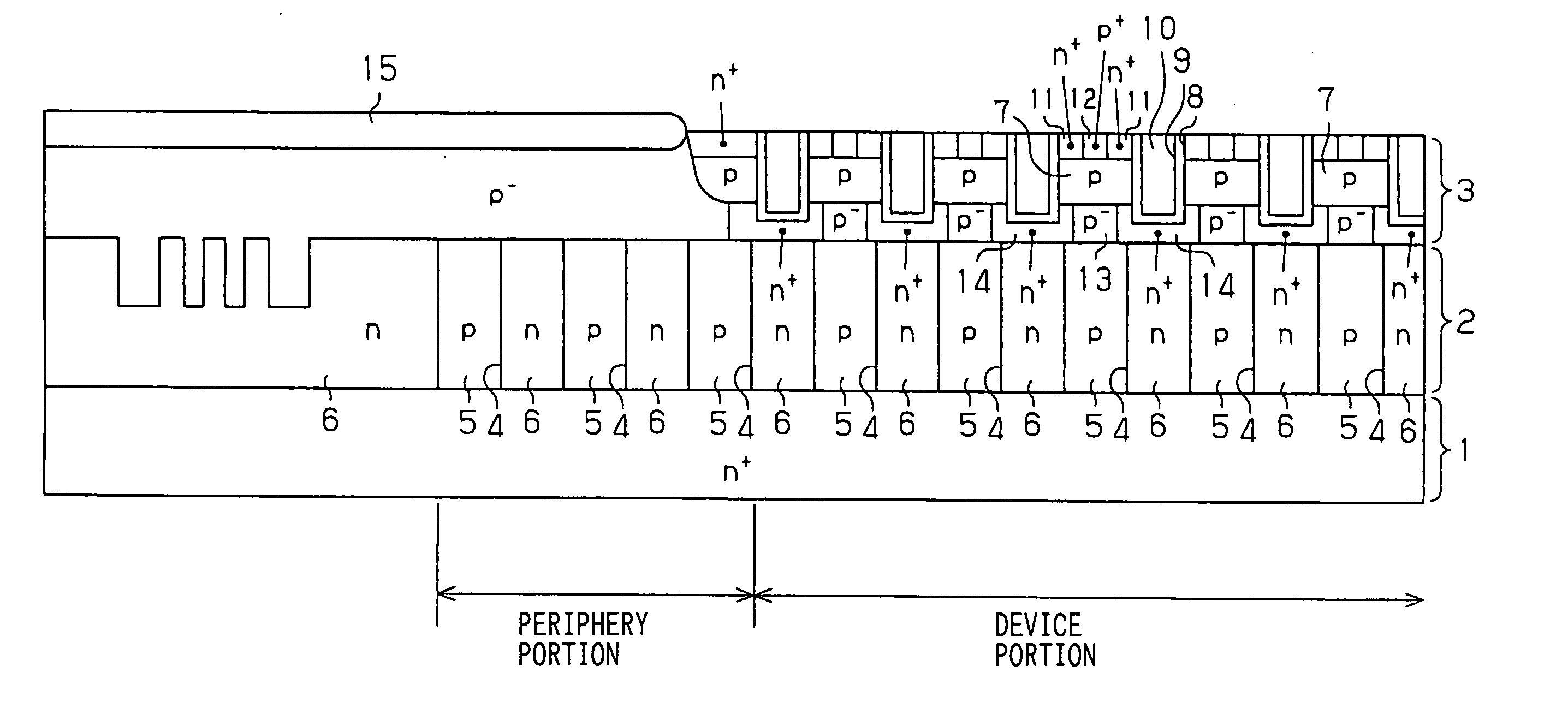
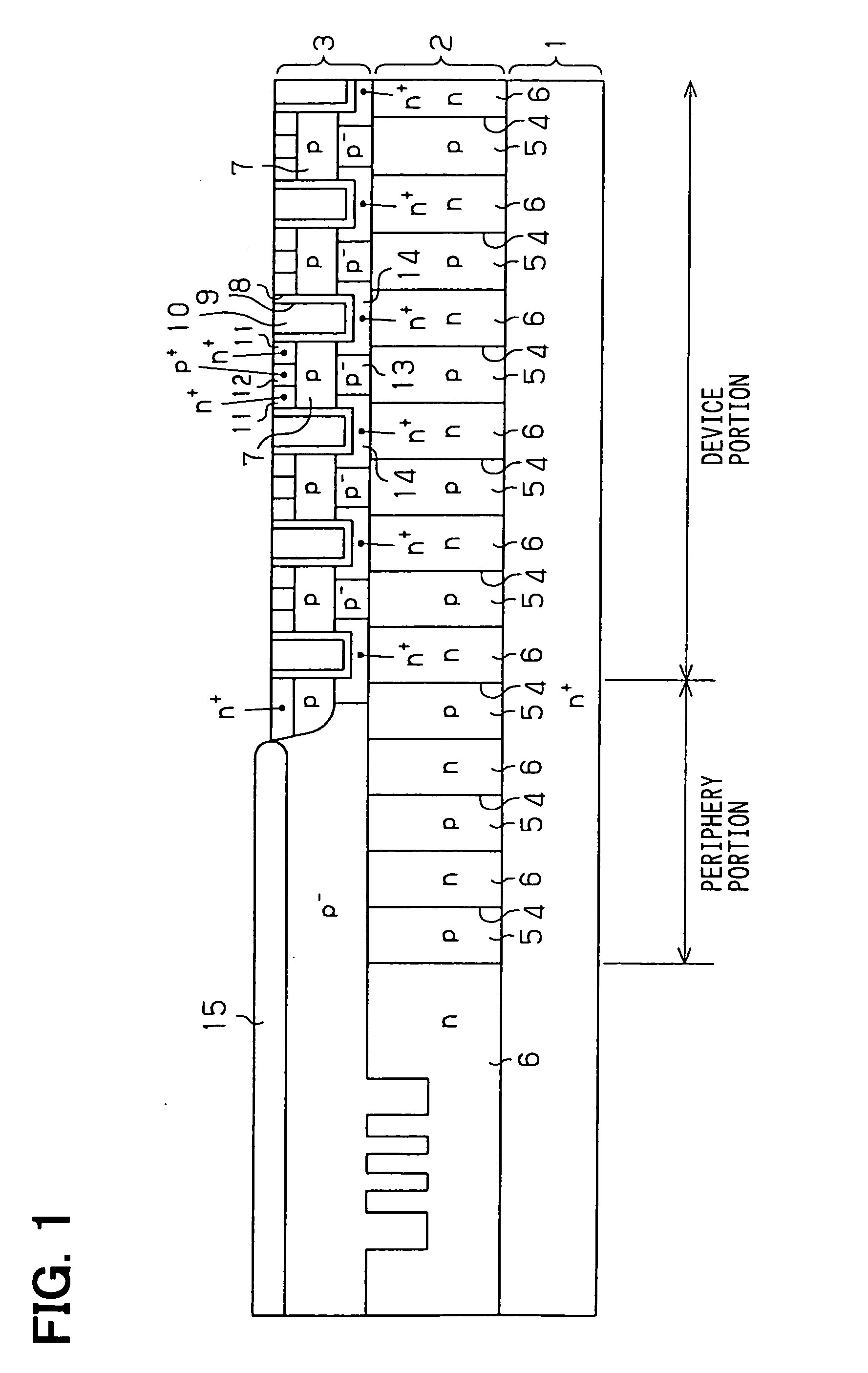
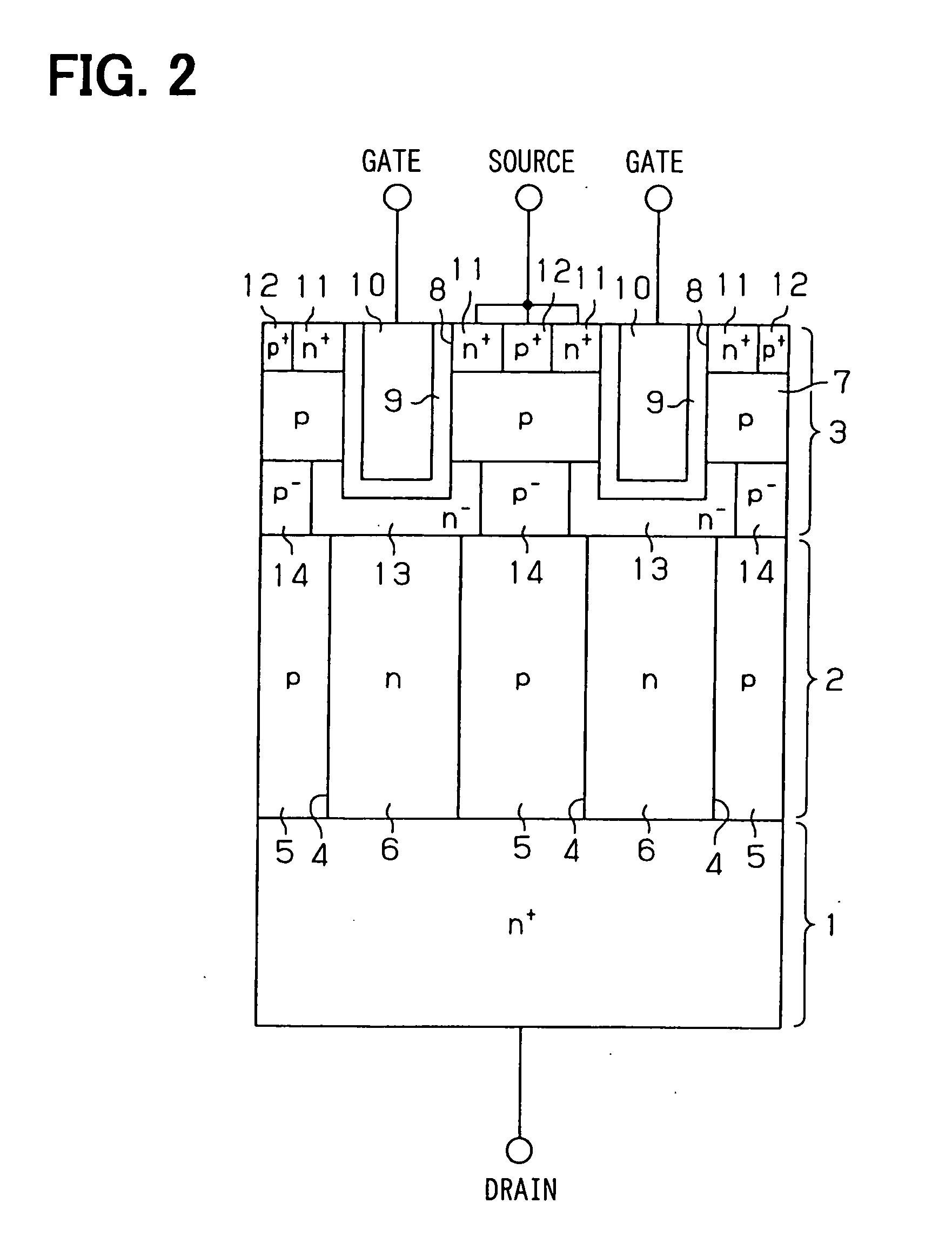

Image

  • Method for manufacturing semiconductor device
  • Method for manufacturing semiconductor device
  • Method for manufacturing semiconductor device

Examples


first embodiment

[0044] The inventors performed a simulation relating to a breakdown voltage when P-type silicon was filled in the trenches of an N-type silicon substrate to form a diode structure. The results of simulation are shown in FIGS. 27A to 27D. FIGS. 27A and 27B show the substrate having void-less structure, and FIGS. 27C and 27D show the substrate having void structure. FIGS. 27A and 27C show electric potential distributions, and FIGS. 27B and 27D show a distribution of an impact ionization ratio. When a defect (i.e., a void) does not occur in an epitaxial film filled in the trenches, a potential distribution and an impact ionization ratio shown in FIGS. 27A and 27B are obtained and a breakdown voltage of 248 V can be secured. However, when a defect (i.e., a void) 101 occurs in the epitaxial film filled in the trenches 102, as shown in FIGS. 27C and 27D, a breakdown occurs at an upper portion 103 of the void 101, which results in reducing a breakdown voltage to 201 V.

[0045] In this manne...

second embodiment

[0110] Next, the second embodiment will be described with a particular emphasis on the difference between the second embodiment and the first embodiment.

[0111] As shown in FIG. 15A, trenches 51 are formed in the silicon substrate 50. Then, as shown in FIG. 15B, an epitaxial film 52 is formed. Further, as shown in FIG. 15C, the epitaxial film 52 is etched by a halogenide gas, whereby the epitaxial film 52 closing the trench openings is removed. Hydrogen chloride (HCl) is used as the halogenide gas.

[0112] Thereafter, as shown in FIG. 15D, an epitaxial film 53 is again formed, thereby being filled in the trenches 51. At this time, the epitaxial film 53 is formed by epitaxial growth using a mixed gas of a silicon source gas and a halogenide gas (the condition [A] in the first embodiment). Further, the epitaxial film 53 may be grown under additional conditions [B] to [E] in the first embodiment.

[0113] The additional etching of the epitaxial film 52 by hydrogen chloride (HCl) can taper...

third embodiment

[0115] Next, the third embodiment will be described with a particular emphasis on the difference between the third embodiment and the first and second embodiments.

[0116]FIGS. 16A to 16D show a process of manufacturing a semiconductor device with a semiconductor substrate of this embodiment. FIGS. 17A to 17D show the relationship between parameters (processing temperature, the amount of flow of a silicon source gas, the amount of flow a halogenide gas, the amount of flow of a dopant gas) when a process of manufacturing (processing) a semiconductor substrate of this embodiment is continuously performed in an epitaxial film forming apparatus. Here, XVIB in FIGS. 17A to 17D represents a process as a doping epitaxial process without halogenide gas shown in FIG. 16B, XVIC in FIGS. 17A to 17D represents a process as a low concentration epitaxial process with the halogenide gas shown in FIG. 16C, and XVID in FIGS. 17A to 17D represents a process as a thermal diffusion process shown in FIG....


PUM


Abstract

A method for manufacturing a semiconductor device includes the steps of: forming a trench in a semiconductor substrate; and forming an epitaxial film on the substrate including a sidewall and a bottom of the trench so that the epitaxial film is filled in the trench. The step of forming the epitaxial film includes a final step before the trench is filled with the epitaxial film. The final step has a forming condition of the epitaxial film in such a manner that the epitaxial film to be formed on the sidewall of the trench has a growth rate at an opening of the trench smaller than a growth rate at a position of the trench, which is deeper than the opening of the trench.

Description

CROSS REFERENCE TO RELATED APPLICATIONS [0001] This application is based on Japanese Patent Applications No. 2004-107859 filed on Mar. 31, 2004, and No. 2004-352010 filed on Dec. 3, 2004, the disclosures of which are incorporated herein by reference. FIELD OF THE INVENTION [0002] The present invention relates to a method for manufacturing a semiconductor device. BACKGROUND OF THE INVENTION [0003] A method for manufacturing a semiconductor device with a semiconductor substrate by which an epitaxial film is filled in trenches to form a doped layer having a high aspect ratio is disclosed in Japanese Patent No. 3485081. Further, a method for manufacturing a semiconductor substrate by which an epitaxial film is filled in trenches to form a doped layer when a super-junction structure (P / N column structure) is formed in a drift region in a vertical type MOS transistor is disclosed in Japanese Unexamined Patent Publication No. 2003-124464. [0004] In the above device, a P-type silicon layer ...

Claims


Application Information

Patent Timeline
Patent Type & Authority Applications(United States)
IPC IPC(8): H01L21/20H01L29/06H01L21/205H01L21/336H01L21/338H01L21/8234H01L29/78
CPCH01L21/823487H01L29/7811H01L29/7813H01L29/0634D06M15/21D06M17/00D06M13/00D06M11/00D06M2200/30
Inventor YAMAUCHI, SHOICHIYAMAGUCHI, HITOSHIMAKINO, TOMOATSUNOGAMI, SYOUJIYAMAOKA, TOMONORI
Owner SUMCO CORP
Why Eureka
Try Eureka