Ultra low-cost uncooled infrared detector arrays in CMOS

a detector array and low-cost technology, applied in the field of uncooled infrared detector arrays in cmos, to achieve the effects of high performance, reduced fabrication process cost, and increased thermal isolation

Inactive Publication Date: 2005-10-13
AKIN TAYFUN
View PDF2 Cites 59 Cited by
  • Summary
  • Abstract
  • Description
  • Claims
  • Application Information

AI Technical Summary

Benefits of technology

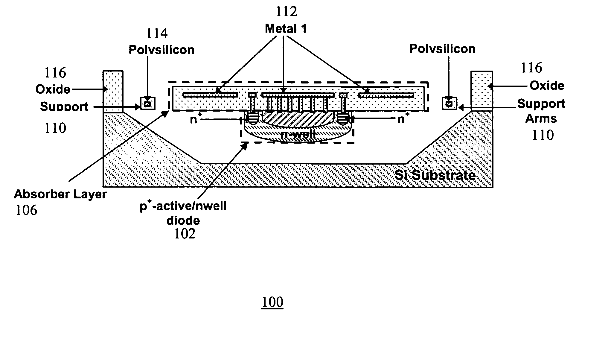
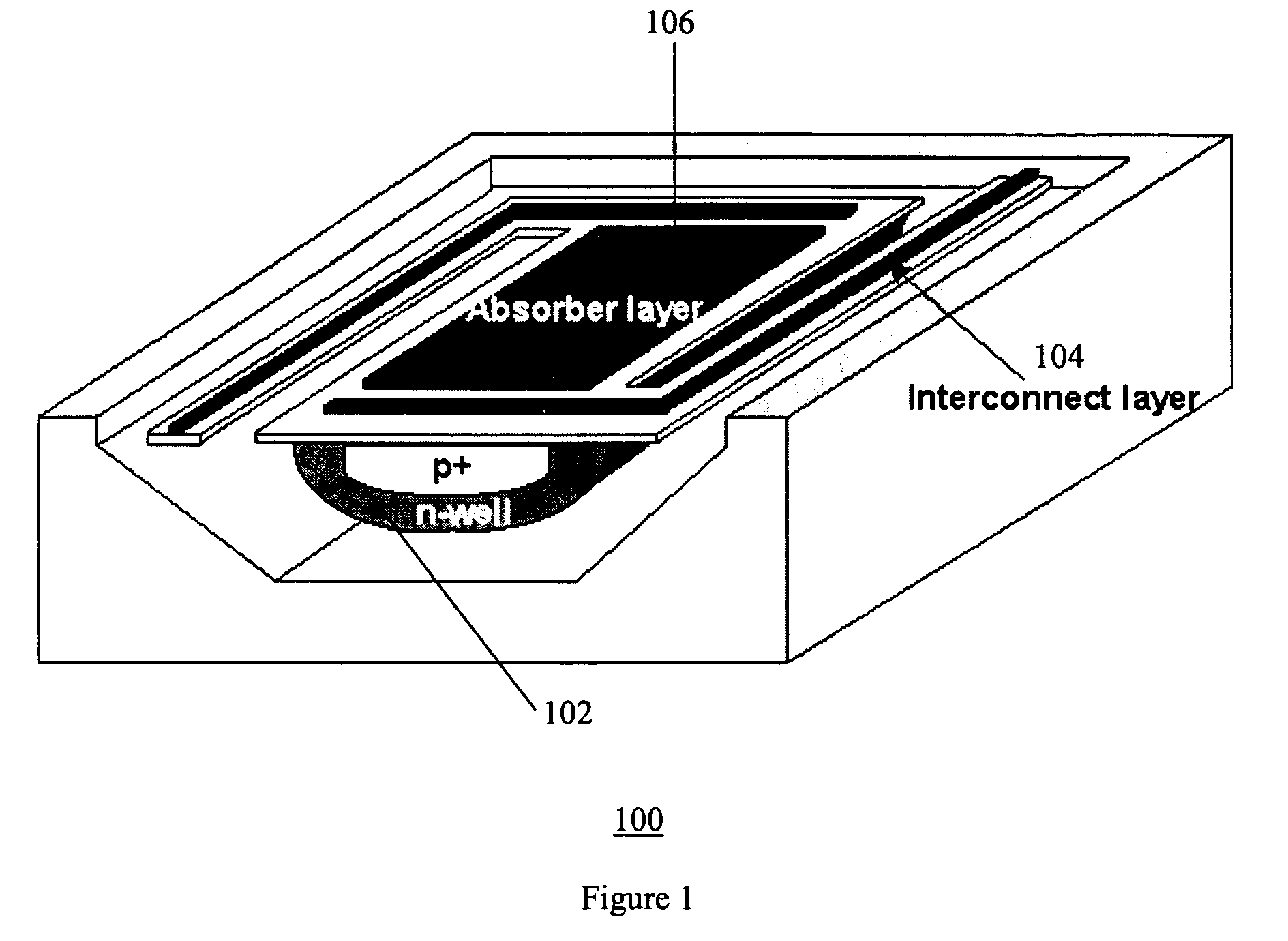
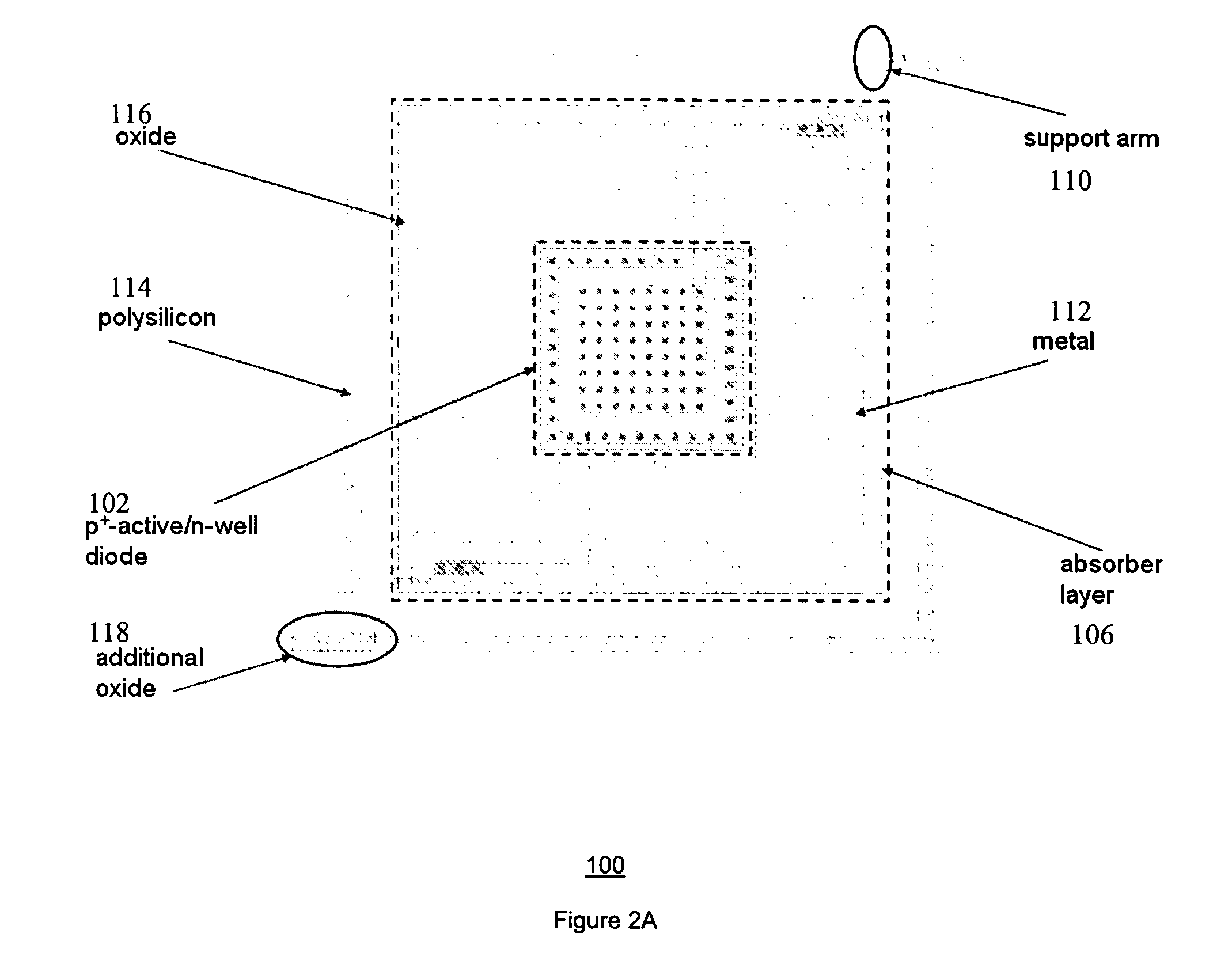
[0020] A post-CMOS processing approach on wafers fabricated using a CMOS process allows the fabrication of a low-cost small pixel size novel detector structure. The detectors in pixels are implemented with p+-active / n-well diodes, which are suspended and thermally isolated from the bulk silicon substrate by etching the silicon underneath the diode using an anisotropic etchant. In order to let the etchant reach the silicon layer to be etched, an RIE step is used to etch the dielectric layers in the CMOS process. Selectively placed CMOS metal layers define the final pixel structure without any lithography, substantially reducing the cost of the fabrication process. The etching of the diode is prevented with electrochemical etch-stop technique. This novel approach is used for first time to implement suspended diode FPAs with standard CMOS technology for uncooled infrared imaging. The detectors have an oxide-metal-oxide sandwich layer on top as the infrared absorbing layer. Other absorber layers can be deposited if higher infrared power absorption is needed. The two support arms allow for the suspension of the diode in each pixel and also carry the electrical signals with an interconnect layer in CMOS. The interconnect layer is selected as a polysilicon layer to increase the thermal isolation between the bulk silicon substrate and the diode in the pixel. The structure to implement the pixel and the post-CMOS process to create the suspended diode arrays are carefully selected to achieve a high performance and low-cost uncooled infrared focal plane arrays. The layout of the pixel and the process steps are very important in order to have small pixel size with high fill factors, good thermal isolation between the suspended diodes and the bulk substrate, low thermal time constant, low thermal mass of the diode structure, high mechanical strength of the supporting arms, and thermal isolation of the pixels from each other to reduce the thermal cross talk.
[0021] With the approach in accordance with the present invention, it is possible to implement large format FPAs such as 128×128 pixels or larger formats with small pixel sizes, such as 40 μm×40 μm with a fill factor of 44%. It will be apparent to those skilled in the art that many different pixel and array sizes can be built using the same sensor structure by slightly modifying the process. The present invention is not in any way restricted by any pixel size or fill factor. The use of diodes as the sensing elements allows achieving very low noise when they are biased at low current. Low biasing current also allows achieving small self heating of the suspended pixel. The selection of a proper value for biasing current for achieving high FPA performance depends on the pixel size, diode area, and the resistance on the interconnect layer. As the bias current increases, the small signal resistance of the diode decreases, decreasing its shot noise current. However, as the current increases, the low frequency noise component in the polysilicon arms increases and there is a reduction in diode temperature coefficient (TC). So there is an optimum operating point for the diode biasing. For the specific FPA mentioned above, the optimum point is around 20 μA, and depending on the CMOS process and diode structure, it can be anywhere between 5 μA and 50 μA.

Problems solved by technology

The main drawback of VOx (R. A. Wood, “Uncooled Thermal Imaging with Monolithic Silicon Focal Arrays,”Infrared Technology XIX, Proc. of SPIE Vol. 2020, pp.
322-329, 1993) is that it is not compatible with CMOS processes and it exhibits large low frequency noise due to its non-crystalline structure, limiting its performance.
CMOS integration is achieved by having a number of deposition, lithography, and etching steps after the CMOS process, increasing the cost of fabrication and reducing yield.
These factors limit the use of infrared detectors with VOx in ultra low-cost applications.
Also, VOx contaminates the CMOS line; therefore, dedicated process equipments and a dedicated cleanroom environment are necessary for the deposition of VOx and any further process step following this deposition step.
276-283, 1999) are CMOS line compatible high TCR materials, i.e., they do not contaminate the CMOS lines; however, they require high temperature annealing to achieve stability of microstructures, making the monolithic CMOS integration difficult.
In addition, both a-Si and poly SiGe have high low frequency noise due to their non-crystalline structures, as VOx.
Futhermore, CMOS integration is also achieved by having a number of depositions, lithography, and etching steps after the CMOS process, increasing the cost of detectors.
However, metal microbolometers not only require deposition and lithography steps after CMOS, but also have low performance due to the low TCR value of metal films.
Since these detectors can not be implemented in a standard CMOS process, it would be difficult to reduce their costs down to limits that ultra low-cost applications require.
In summary, none of the previous approaches provide a good solution for ultra low-cost uncooled infrared detector arrays, as they have one or more of the following drawbacks: (i) They use high TCR materials that are not CMOS line compatible, requiring dedicated additional equipment; (ii) They use high TCR materials that are not CMOS process compatible, making the integration with CMOS circuit difficult; (iii) They require complicated post-CMOS processes including a number of critical lithography, deposition, and etching steps; (iv) They require dedicated in house CMOS processes with non standard CMOS process steps.
Although the approach can be used to create large format infrared FPAs, the use of surface micromachining and VOx material does not allow implementing ultra low-cost infrared FPAs as explained above in opposition to public disclosure document (R. A. Wood, “Uncooled Thermal Imaging with Monolithic Silicon Focal Arrays,”Infrared Technology XIX, Proc. of SPIE Vol. 2020, pp.
However, Reay et al fail to realize that the diodes cannot be used to implement high performance uncooled infrared focal plane arrays.
With the current sub-micron CMOS processes, the suggested method of achieving exposed silicon substrate does not work, as the dielectric and other layer thicknesses are large.
However, when these additives are added, then the undercut of the opening areas is going to increase, and therefore, the walls between the pixels will be etched, causing pixel cross-talk.
A high degree of pixel cross-talk prevents making good quality Focal Plane Arrays (FPA).
This process, however, will reduce the fill factor of the pixel in the FPA, reducing the efficiency.
In summary, the suggested methods in U.S. Pat. No. 5,600,174 by Reay et al will not achieve the performance necessary for creation of large format low-cost uncooled infrared detector focal plane arrays.
However the use of isotropic wet etching after the dry etching cannot be used to implement diode type uncooled infrared detector FPAs.
Isotropic wet etching cannot be used with electrochemical etch-stop to achieve suspended diode structures.
Furthermore, isotropic wet etching removes the sidewalls, increasing the thermal cross-talk between the pixels of the FPA and decreasing the mechanical strength of the FPA.
If the width of the sidewalls are made large to prevent their entire etching, then the pixel fill factor will reduce and pixel size will increase, both of which are not desired to achieve low-cost, high performance uncooled infrared detector FPAs.

Method used


Image

  • Ultra low-cost uncooled infrared detector arrays in CMOS
  • Ultra low-cost uncooled infrared detector arrays in CMOS
  • Ultra low-cost uncooled infrared detector arrays in CMOS

Examples


Embodiment Construction

[0032] The present invention relates to uncooled infrared detector arrays in CMOS. The following description is presented to enable one of ordinary skill in the art to make and use the invention and is provided in the context of a patent application and its requirements. Various modifications to the preferred embodiments and the generic principles and features described herein will be readily apparent to those skilled in the art. Thus, the present invention is not intended to be limited to the embodiments shown, but is to be accorded the widest scope consistent with the principles and features described herein.

[0033] In accordance with the present invention, a microbolometer infrared sensor pixel design and sensor array design compatible with CMOS process is described. The pixel design and the resulting sensor array does not require any critical post-CMOS lithography and complex deposition processes that increase fabrication costs and reduce yield. The invention makes it possible b...


PUM


Abstract

Micromachined, CMOS p+-active / n-well diodes are used as infrared sensing elements in uncooled Focal Plane Arrays (FPA). The FPAs are fabricated using a standard CMOS process followed by post-CMOS bulk-micromachining steps without any critical lithography or complicated deposition processes. Micromachining steps include Reactive Ion Etching (RIE) to reach the bulk silicon and anisotropic silicon wet etching together with electrochemical etch-stop technique to obtain thermally isolated p+-active / n-well diodes. The FPAs are monolithically integrated with their readout circuit since they are fabricated in any standard CMOS technology.

Description

FIELD OF THE INVENTION [0001] The present invention relates to uncooled infrared detector arrays in CMOS. More specifically, this invention relates to suspended and thermally isolated CMOS p+-active / n-well diodes used as infrared sensing elements in uncooled infrared detector arrays. The elements are manufactured using silicon micro-machining of CMOS processed chips / wafers with Micro Electro Mechanical Systems (MEMS) technology. BACKGROUND OF THE INVENTION [0002] Uncooled infrared detectors have recently gained wide attention for infrared imaging applications, due to their advantages such as low cost, low weight, low power, wide spectral response, and long term operation compared to those of photon detectors. Uncooled technology has great potential for use in various civilian applications, like driver's night vision enhancement, security cameras, heat analysis, mine detection, and fire detection. Worldwide effort is still continuing to implement very large format arrays at low cost....

Claims


Application Information

Patent Timeline
Patent Type & Authority Applications(United States)
IPC IPC(8): G01J5/20H01L27/146
CPCG01J5/20H01L27/14603H01L27/1463H01L27/14649
Inventor AKIN, TAYFUNEMINOGLU, SELIMTANRIKULU, M. YUSUF
Owner AKIN TAYFUN
Why Eureka
Try Eureka