Semiconductor device and its manufacturing method

a technology of semiconductor devices and manufacturing methods, applied in semiconductor devices, diodes, electrical devices, etc., can solve the problems of inadequacy, low yield, and complicated manufacturing processes, and achieve the effect of simplifying the process

Inactive Publication Date: 2005-10-13
FUJITSU LTD
View PDF2 Cites 120 Cited by
  • Summary
  • Abstract
  • Description
  • Claims
  • Application Information

AI Technical Summary

Benefits of technology

[0039] An object of this invention is to provide a semiconductor device manufacture method capable of forming transistors and resistors by simplified processes.

Problems solved by technology

If transistors and other elements are integrated by independent processes, the manufacture processes become complicated and a yield lowers.
If the resistance value is too high or low, this is not appropriate in many cases.
However, only one operation voltage is often used for middle voltage transistors requested by particular customers.
If an independent manufacture process matching the desired characteristics of each transistor is selected when a plurality kind of transistors are integrated, the number of processes increases and the manufacture processes become complicated, resulting in a lowered yield and a high manufacture cost.

Method used


Image

  • Semiconductor device and its manufacturing method
  • Semiconductor device and its manufacturing method
  • Semiconductor device and its manufacturing method

Examples


Embodiment Construction

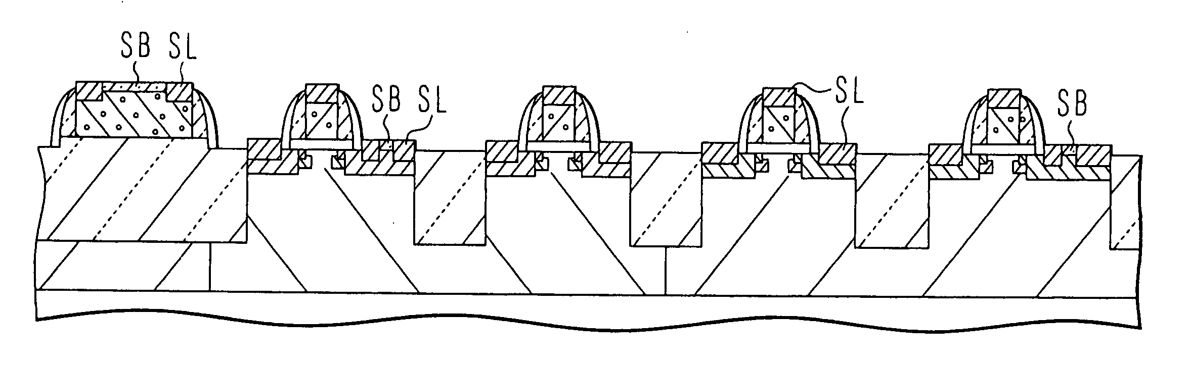
[0064] The present inventors are now under developments of a semiconductor device which mounts, on the same chip, low voltage transistors including SRAM, a flash memory, high voltage transistors for controlling the flash memory, middle voltage transistors for an ultra high speed input / output circuit, high precision resistors for an analog circuit, diffusion resistors for ESD protection, by photolithography of the 0.13 μm rule.

[0065] First, description will be made on the analysis, made by the present inventors, of the technologies disclosed in Japanese Patent Laid-open Publication No. 2000-164727.

[0066] Japanese Patent Laid-open Publication No. 2000-164727 concludes that even if phosphorus (P+) ions are implanted into the gate insulating film having a thickness of 20 nm at an acceleration energy of 10 keV to 30 keV and a dose of 2×1013 cm−2 to 5×1013 cm−2, the implanted P+ ions will not reach the silicon substrate.

[0067]FIG. 12 is a graph showing an impurity concentration distrib...


PUM


Abstract

A semiconductor device manufacturing method includes, forming isolation region having an aspect ratio of 1 or more in a semiconductor substrate, forming a gate insulating film, forming a silicon gate electrode and a silicon resistive element, forming side wall spacers on the gate electrode, heavily doping a first active region with phosphorus and a second active region and the resistive element with p-type impurities by ion implantation, forming salicide block at 500° C. or lower, depositing a metal layer covering the salicide block, and selectively forming metal silicide layers. The method may further includes, forming a thick and a thin gate insulating films, and performing implantation of ions of a first conductivity type not penetrating the thick gate insulating film and oblique implantation of ions of the opposite conductivity type penetrating also the thick gate insulating film before the formation of side wall spacers.

Description

CROSS REFERENCE TO RELATED APPLICATION [0001] This application is a continuation application of International Patent Application PCT / JP2003 / 007384 filed on Jun. 10, 2003, the entire contents of which are incorporated herein by reference.BACKGROUND OF THE INVENTION [0002] A) Field of the Invention [0003] The present invention relates to a semiconductor device and its manufacture method, and more particularly to a semiconductor device having a plurality of semiconductor elements such as micro transistors and resistors or a plurality of transistors operating at different voltages, a semiconductor device having transistors with improved breakdown voltages, and their manufacture methods. [0004] B) Description of the Related Art [0005] As the integration degree of semiconductor integrated circuit devices (IC) is improved, transistors as IC constituent elements are made very fine. The performance of logic semiconductor elements has improved considerably and many functions are fabricated on...

Claims


Application Information

Patent Timeline
Patent Type & Authority Applications(United States)
IPC IPC(8): H01L21/8238H01L27/06
CPCH01L21/823857H01L27/0629H01L21/823892
Inventor EMA, TAIJIKOJIMA, HEDEYUKIANEZAKI, TORU
Owner FUJITSU LTD
Why Eureka
Try Eureka