Light-emitting semiconductor device, light-emitting system and method for fabricating light-emitting semiconductor device

Inactive Publication Date: 2005-10-13
PANASONIC CORP
View PDF99 Cites 71 Cited by
  • Summary
  • Abstract
  • Description
  • Claims
  • Application Information

AI Technical Summary

Benefits of technology

[0074] If the substantial thickness of the luminescent layer is set within the range from 50 μm to 1000 μm, both inclusive, and more preferably within the range from 100 μm to 700 μm, both inclusive, the cross-sectional area of the silicate phosphor to be excited by the blue light increases, as compared to the case of the known YAG phosphor. Accordingly, the luminous intensity of the yellow light emitted by the silicate phosphor increases, and the light-emitting semiconductor device emits white light with excellent color tone by adding the colors the yellow light and of the blue light emitted by the blue-light-emitting device together. Moreover, as described above, since the luminescent layer has substantially no light absorption and attenuation factor, blue light emitted by a blue-light-emitting device either passes through the luminescent layer without being absorbed and attenuated or contributes to excitation of the phosph

Problems solved by technology

However, an additional examination done by the present inventors proved that such a structure cannot be formed in reality by the pouring technique described above using a YAG-based phosphor and the disclosed resin (e.g., epoxy resin, urea resin or silicon).
Accordingly, the resultant substantial luminescent layer is not in the state in which the YAG-based phosphor particles are scattered throughout the base material, resulting in causing uneven distribution of phosphor particles in the package.
In addition, the resultant luminescent layer exhibits a low luminescence performance.
In a light-emitting semiconductor device using a blue LED and a phosphor in combination, color unevenness in emission of light has been a problem and various measurements have taken to suppress the color unevenness.
The reason of this distribution unevenness is not clear but the difference in specific gravity between the phosphor and the base material is at least one cause of the distribution unevenness.
It should be noted that the phosphor not only has a low emission efficiency when irradiated with blue light (excitation light) but also contains noxious Cd, and therefore the phosphor is difficult to, for example, fabricate, handle and storage.
Therefore, since the known light-emitting semiconductor devices exhibit distribution unevenness of phosphor particles in luminescent layers, the devices have a problem that unevenness is created in emission of light to cause low fabrication yields.
This problem of emission unevenness is commonly observed among the known light-emitting semiconductor devices configured by using YAG-based phosphors, and also observed in light-emitting semiconductor devices additionally using red phosphors to compensate f

Method used


Image

  • Light-emitting semiconductor device, light-emitting system and method for fabricating light-emitting semiconductor device
  • Light-emitting semiconductor device, light-emitting system and method for fabricating light-emitting semiconductor device
  • Light-emitting semiconductor device, light-emitting system and method for fabricating light-emitting semiconductor device

Examples


embodiment 1

[0164] Hereinafter, a first embodiment of the present invention relating to a light-emitting semiconductor device and a method for suppressing color unevenness in the light-emitting semiconductor device will be described with reference to the drawings.

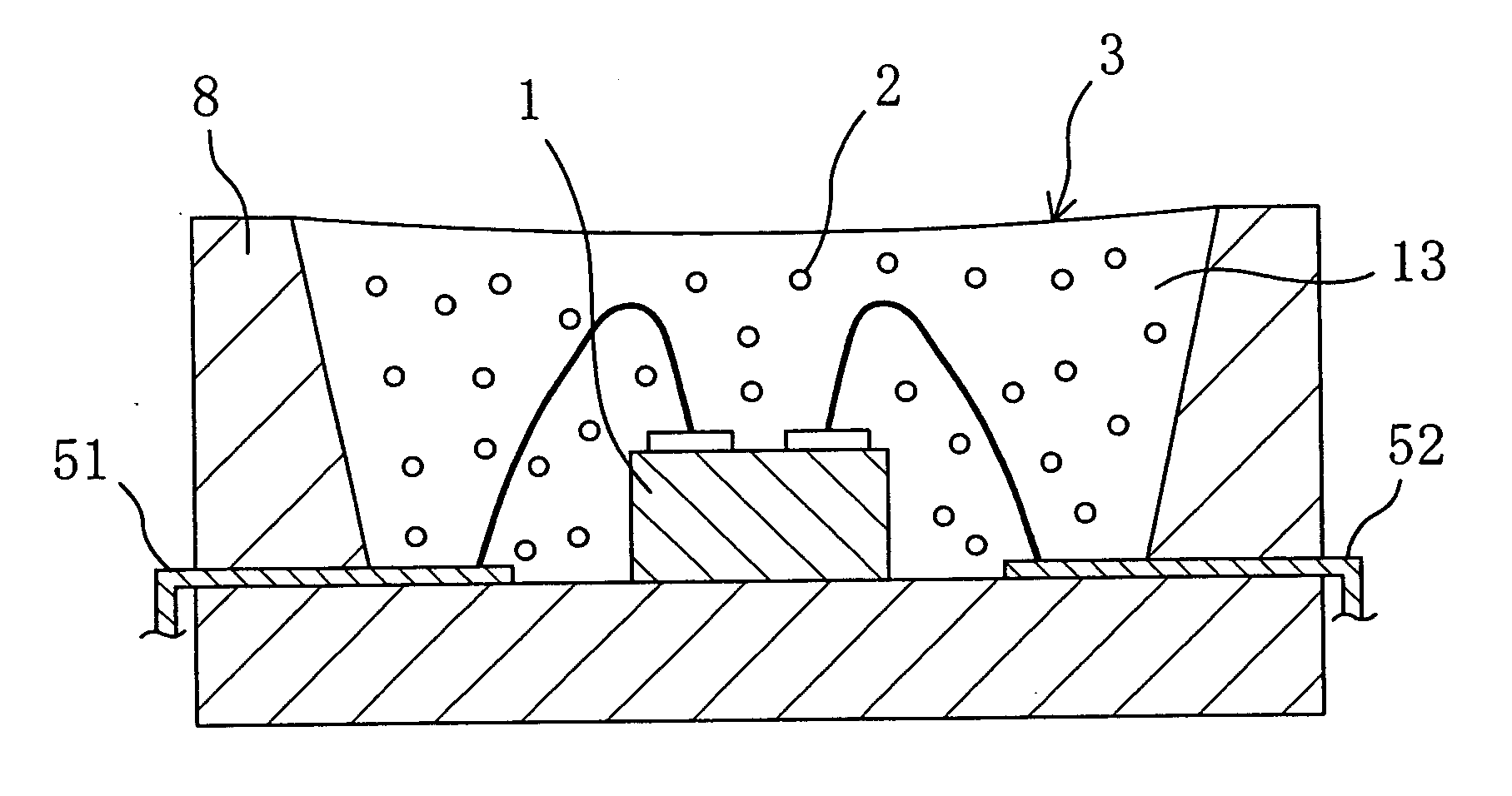
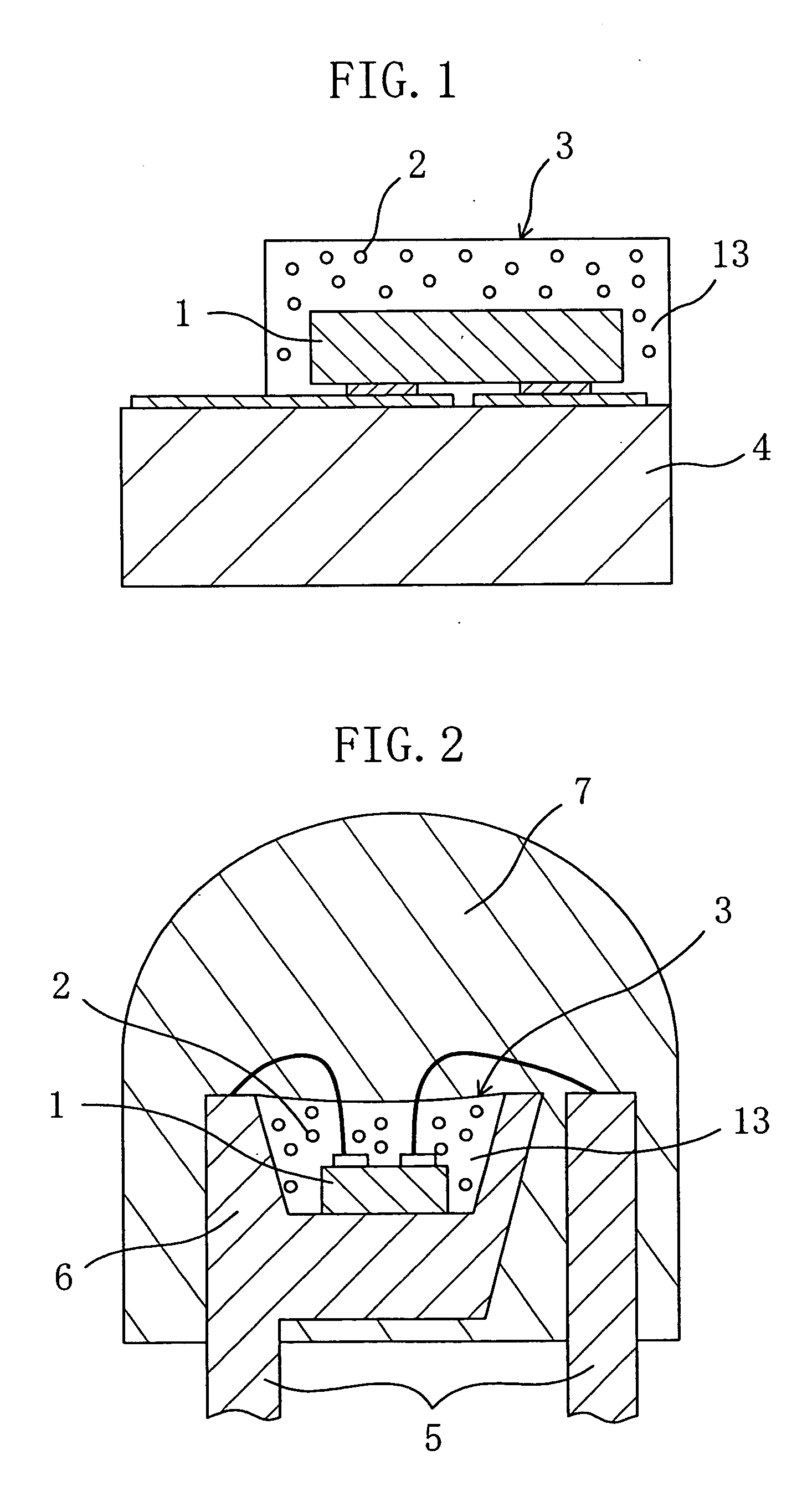
[0165]FIG. 1 is a vertical cross-sectional view showing a first exemplary light-emitting semiconductor device as a relatively typical example of this embodiment. As shown in FIG. 1, the first exemplary light-emitting semiconductor device is a chip-type light-emitting semiconductor device including: a substrate 4 (a submount element) functioning as a Zener diode; a flip-chip-type blue LED 1 mounted on the substrate 4 to be electrically connected to the Zener diode in the substrate; and a luminescent layer 3 encapsulating the blue LED 1 and made of a mixture of yellow / yellowish phosphor particles 2 and a base material 13 (a translucent resin). The blue LED 1 has a main light-extracting surface facing upward as shown in FIG. 1. The lumin...

embodiment 2

[0239] Now, an embodiment of a light-emitting system according to the present invention is described with reference to the drawings.

[0240] Various kinds of displaying systems using light-emitting semiconductor devices (e.g., LED information display terminals, LED traffic lights, LED stoplights of vehicles and LED directional lights) and various kinds of lighting systems (e.g., LED interior / exterior lights, courtesy LED lights, LED emergency lights, and LED surface emitting sources) are herein defined broadly as light-emitting systems.

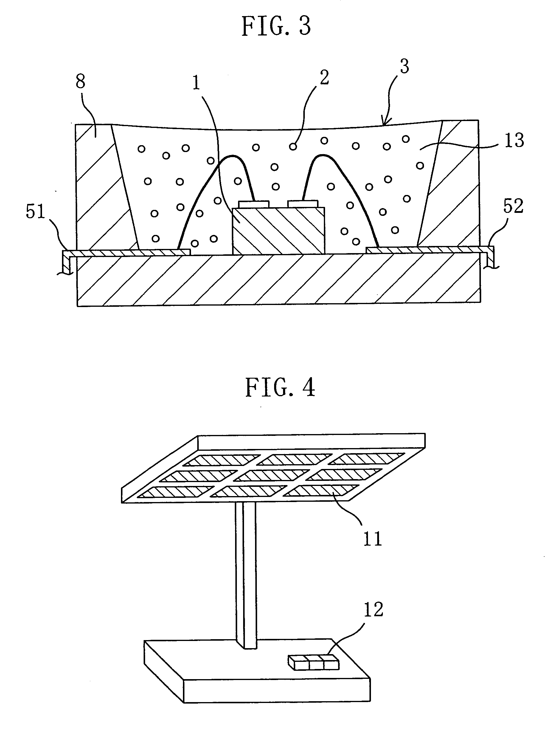
[0241]FIGS. 4 through 6 are perspective views respectively showing examples of a light-emitting system according to a second embodiment of the present invention. FIG. 4 is a perspective view schematically showing a configuration of a desk-lamp-type lighting system as a first exemplary light-emitting system of the present invention.

[0242] As shown in FIG. 4, the first exemplary light-emitting system includes: a lighting unit in which a large number of...

embodiment 3

[0427] In this embodiment, a method for forming a thin luminescent layer is described. According to this embodiment, yellow / yellowish phosphor particles which are expressed by the chemical formula (Sr1-a1-b1-xBaa1Cab1Eux)2SiO4 where the values a1, b1 and x are in the ranges 0≦a1≦0.3, 0≦b1≦0.8 (more preferably 0≦b1≦0.6) and 0

[0428] Hereinafter, examples of the fabrication method will be de...


PUM


Abstract

A chip-type light-emitting semiconductor device includes: a substrate 4; a blue LED 1 mounted on the substrate 4; and a luminescent layer 3 made of a mixture of yellow/yellowish phosphor particles 2 and a base material 13 (translucent resin). The yellow/yellowish phosphor particles 2 is a silicate phosphor which absorbs blue light emitted by the blue LED 1 to emit a fluorescence having a main emission peak in the wavelength range from 550 nm to 600 nm, inclusive, and which contains, as a main component, a compound expressed by the chemical formula: (Sr1-a1-b1-xBaa1Cab1Eux)2SiO4 (0≦a1≦0.3, 0≦b1≦0.8 and 0<x<1). The silicate phosphor particles disperse substantially evenly in the resin easily. As a result, excellent white light is obtained.

Description

TECHNICAL FIELD [0001] The present invention relates to light-emitting semiconductor devices utilizing blue-light-emitting diodes (hereinafter, referred to as blue LEDs) and yellow / yellowish phosphors in combination to emit white light, light-emitting systems using the light-emitting semiconductor devices, and methods for fabricating the light-emitting semiconductor devices. BACKGROUND ART [0002] A light-emitting semiconductor device utilizing a blue LED (strictly speaking, a blue LED chip) having a main emission peak in the blue wavelength range from 400 nm to 530 nm, both inclusive, and a luminescent layer containing an inorganic phosphor (hereinafter, simply referred to as a “phosphor”) that absorbs blue light emitted by the blue LED and produces a fluorescence having an emission peak within a visible wavelength range from green to yellow (in the range of about 530 nm to about 580 nm) in combination is known to date. Light emitted from an LED that excites a phosphor is herein ref...

Claims


Application Information

Patent Timeline
IPC IPC(8): H01L33/32H01L33/50H01L33/56H01L33/60H01L33/62
CPCC09K11/025H01L24/45C09K11/7734C09K11/7735C09K11/7774C09K11/7792F21S6/00F21S6/003F21Y2101/02H01L33/502H01L33/54H05B33/14Y02B20/181C09K11/7731H01L2924/12041H01L2224/8592H01L2224/48257H01L2224/73265H01L2224/48247H01L2224/48227H01L2224/48091H01L2224/32225H01L2224/16145H01L2224/45144H01L2224/45124H01L2924/00014H01L2924/00H01L2924/12035H01L2924/12042H01L2924/12044H01L2924/181F21Y2115/10Y02B20/00C09K11/77342H01L2924/00012
Inventor MAEDA, TOSHIHIDEOSHIO, SHOZOIWAMA, KATSUAKIKITAHARA, HIROMIIKEDA, TADAAKIKAMEI, HIDENORIHANADA, YASUYUKISAKANOUE, KEI
Owner PANASONIC CORP
Why Eureka
Try Eureka