Ferroelectric memory device and method of manufacturing the same

a technology of ferroelectric memory and ferroelectric technology, which is applied in the direction of digital storage, semiconductor devices, instruments, etc., can solve the problems of ferroelectric crystallinity impairment, electrical characteristics deterioration to a considerable extent, and hydrogen to be generated as a reaction by-produ

Inactive Publication Date: 2005-10-20
SEIKO EPSON CORP
View PDF8 Cites 11 Cited by
  • Summary
  • Abstract
  • Description
  • Claims
  • Application Information

AI Technical Summary

Benefits of technology

[0004] In general, when using the above-mentioned oxide material as a capacitor insulating layer, an interlayer dielectric such as SiO2 is deposited after forming an upper electrode in order to provide electrical insulation between each memory element as the major objective. As the deposition method, a chemical vapor deposition (CVD) method excelling in step coverage is generally used. However, use of such a deposition method causes hydrogen to be generated as a reaction by-product. In particular, if activated hydrogen passes through SiO2 and the upper electrode and reaches the ferroelectric thin film, the crystallinity of the ferroelectric is impaired due to the reducing effect of hydrogen, whereby the electrical characteristics deteriorate to a considerable extent. The characteristics of a MOS transistor as a switching element deteriorate due to lattice defects occurring in the silicon single crystal during the device manufacturing step. Therefore, it is necessary to subject the MOS transistor to a heat treatment in a hydrogen-containing nitrogen gas in the final stage. However, since the hydrogen concentration in this step is higher than that during formation of the interlayer dielectric, damage occurring to the ferroelectric thin film is more acute.

Problems solved by technology

However, use of such a deposition method causes hydrogen to be generated as a reaction by-product.
In particular, if activated hydrogen passes through SiO2 and the upper electrode and reaches the ferroelectric thin film, the crystallinity of the ferroelectric is impaired due to the reducing effect of hydrogen, whereby the electrical characteristics deteriorate to a considerable extent.
The characteristics of a MOS transistor as a switching element deteriorate due to lattice defects occurring in the silicon single crystal during the device manufacturing step.
However, since the hydrogen concentration in this step is higher than that during formation of the interlayer dielectric, damage occurring to the ferroelectric thin film is more acute.
Specifically, once the ferroelectric capacitor is covered with the hydrogen barrier film, it is extremely difficult to recover the crystallinity of the ferroelectric to secure the electrical characteristics of the capacitor.
However, damage to the ferroelectric often occurs during formation of the ferroelectric capacitor.
However, if hydrogen generated during the resist combustion process, a water molecule, or a reducing etching gas passes through the upper electrode and reaches the interface between the upper electrode and the ferroelectric, the ferroelectric is reduced in this region, whereby the crystallinity is impaired to a considerable extent.
Since such damage cannot be sufficiently corrected by subsequent heating and is more sensitive to the reducing atmosphere in the subsequent step, the crystallinity is easily disordered.
Therefore, a damaged region which cannot contribute to polarization switching occurs.
In particular, a minute capacitor cannot exhibit sufficient characteristics.

Method used


Image

  • Ferroelectric memory device and method of manufacturing the same
  • Ferroelectric memory device and method of manufacturing the same
  • Ferroelectric memory device and method of manufacturing the same

Examples


first embodiment

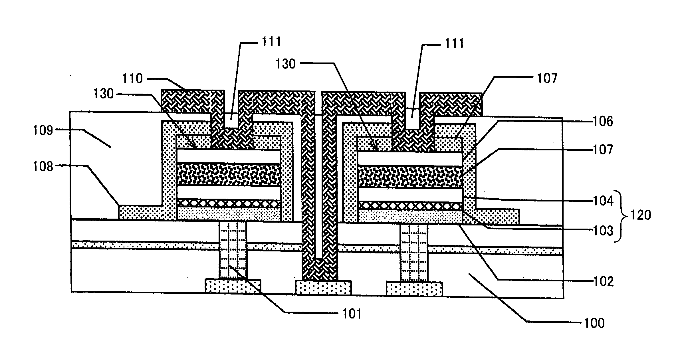
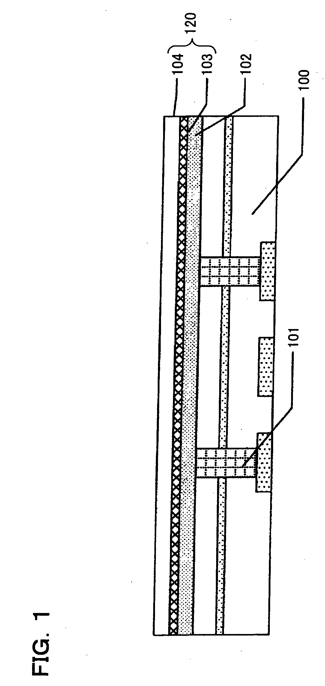
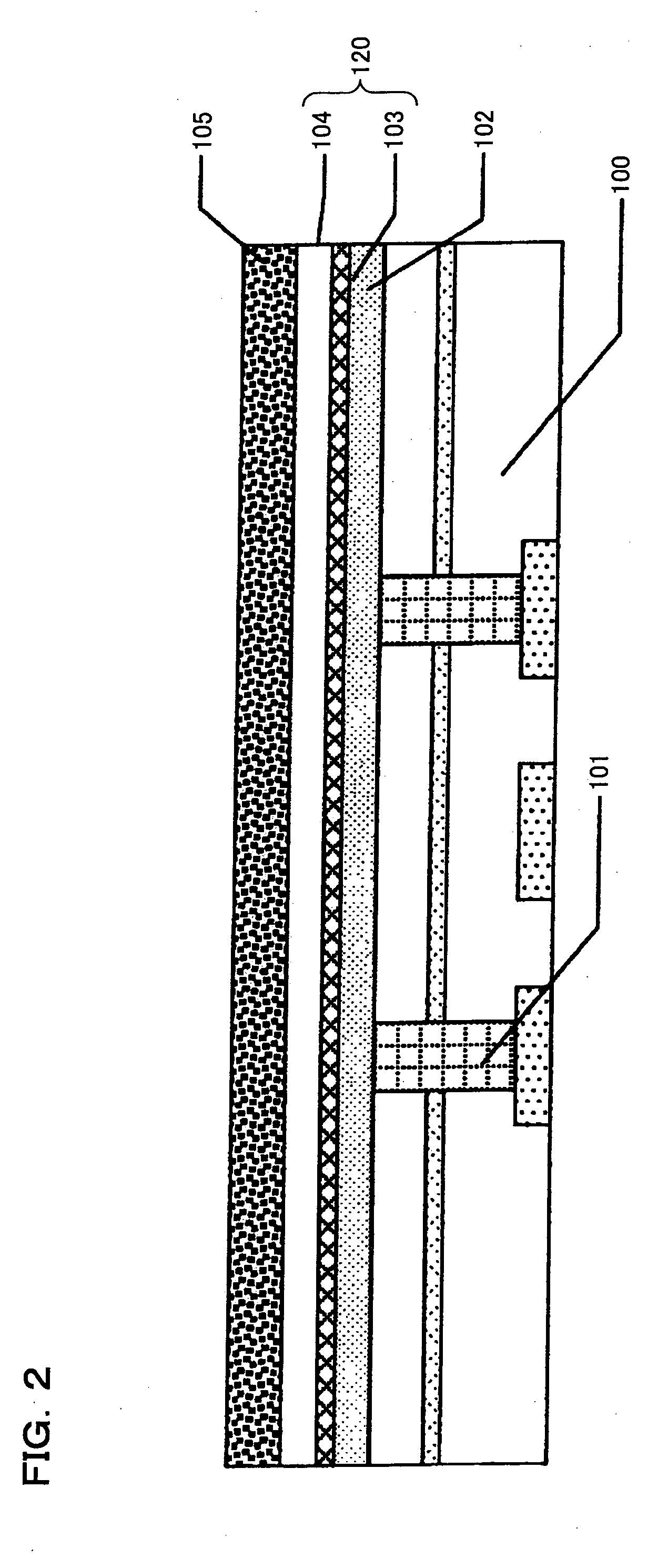
[0133] FIGS. 1 to 11 schematically show a method of manufacturing a ferroelectric memory device according to a first embodiment of the present invention.

[0134] (1) As shown in FIG. 1, a plug 101 is formed in a substrate 100, and a barrier metal layer 102 and a lower electrode 120 are formed on the plug 101.

[0135] A resist pattern for forming a contact hole is formed by a lithographic step on the substrate 100 on which a switching transistor is formed, and a contact hole is formed by using a dry etching method. After depositing a conductive film (tungsten film, for example) by using a chemical vapor deposition (CVD) method, the conductive film is ground by chemical mechanical polishing to form the plug (tungsten plug, for example) 101 in the contact hole. The substrate 100 includes a semiconductor substrate and an interlayer dielectric formed on the semiconductor substrate.

[0136] A titanium aluminum nitride (TiAlN) film is deposited as the barrier metal layer 102 by using a sputte...

second embodiment

[0171] FIGS. 16 to 26 schematically show a method of manufacturing a ferroelectric memory device according to a second embodiment of the present invention. In this embodiment, the patterning step of the upper electrode 206 is separately performed from the patterning step of the ferroelectric film 204, the lower electrode 220, and the barrier metal layer 202.

[0172] (1) As shown in FIG. 16, a plug 201 is formed in a substrate 200, and a barrier metal layer 202 and a lower electrode 220 are formed on the plug 201. The details are the same as described for the first embodiment. The lower electrode 220 may be formed by stacking an iridium (Ir) thin film 203 and a platinum (Pt) film 204.

[0173] (2) As shown in FIGS. 17 to 19, a ferroelectric film 205 and an upper electrode 206 are formed on the lower electrode 220.

[0174] The material and the deposition method for the ferroelectric film 205 and the upper electrode 206 are the same as described for the first embodiment. However, in this e...

third embodiment

[0198] FIGS. 29 to 41 schematically show a method of manufacturing a ferroelectric memory device according to a third embodiment of the present invention. In this embodiment, a third hydrogen barrier film 309 is formed in addition to first and second hydrogen barrier films 307 and 308.

[0199] (1) As shown in FIG. 29, a plug 301 is formed in a substrate 300, and a barrier metal layer 302 and a lower electrode 320 are formed on the plug 301. The details are the same as described in the first embodiment. The lower electrode 320 may be formed by stacking an iridium (Ir) thin film 303 and a platinum (Pt) film 304.

[0200] (2) As shown in FIGS. 30 and 31, a ferroelectric film 305 and an upper electrode 306 are formed on the lower electrode 320. The material and the deposition method for the ferroelectric film 305 and the upper electrode 306 are the same as described in the first embodiment.

[0201] (3) As shown in FIG. 32, the first hydrogen barrier film 307 is formed on the upper electrode...


PUM

PropertyMeasurementUnit
thicknessaaaaaaaaaa
thicknessaaaaaaaaaa
thicknessaaaaaaaaaa

Abstract

A ferroelectric memory device includes: a substrate; a ferroelectric capacitor which is formed on the substrate and includes a lower electrode, a ferroelectric film, and an upper electrode; a hydrogen barrier film provided to cover the ferroelectric capacitor; and an interlayer dielectric provided on the hydrogen barrier film. A thickness of an area of the hydrogen barrier film provided on the upper electrode is greater than a thickness of an area of the hydrogen barrier film provided on a sidewall of the ferroelectric capacitor.

Description

[0001] Japanese Patent Application No. 2004-087622, filed on Mar. 24, 2004, and Japanese Patent Application No. 2005-005341, filed on Jan. 12, 2005 are hereby incorporated by reference in their entireties. BACKGROUND OF THE INVENTION [0002] The present invention relates to a ferroelectric memory device and a method of manufacturing the same. [0003] A nonvolatile memory device using spontaneous polarization specific to a ferroelectric (ferroelectric memory device) has attracted attention as an ultimate memory having the possibility of replacing not only a conventional nonvolatile memory but also most memories such as a static RAM (SRAM) and a DRAM due to its characteristics such as a high-speed write / read and low-voltage operation. As the ferroelectric material, a number of candidate materials have been proposed. In particular, a perovskite-type oxide such as lead zirconate titanate (Pb(Zr,Ti)O3 hereinafter abbreviated as “PZT”) and a bismuth-layered compound such as SrBi2Ta2O9 are c...

Claims


Application Information

Patent Timeline
Patent Type & Authority Applications(United States)
IPC IPC(8): G11C11/22H01L21/768H01L21/82H01L21/8246H01L27/10H01L27/105H01L27/108H01L27/115H01L29/76
CPCG11C11/22H01L27/11507H01L27/11502H10B53/00H10B53/30
Inventor TAMURA, HIROAKITAGAWA, TERUO
Owner SEIKO EPSON CORP
Why Eureka
Try Eureka