Semiconductor device, mask for impurity implantation, and method of fabricating the semiconductor device
- Summary
- Abstract
- Description
- Claims
- Application Information
AI Technical Summary
Benefits of technology
Problems solved by technology
Method used
Image

Examples
first embodiment
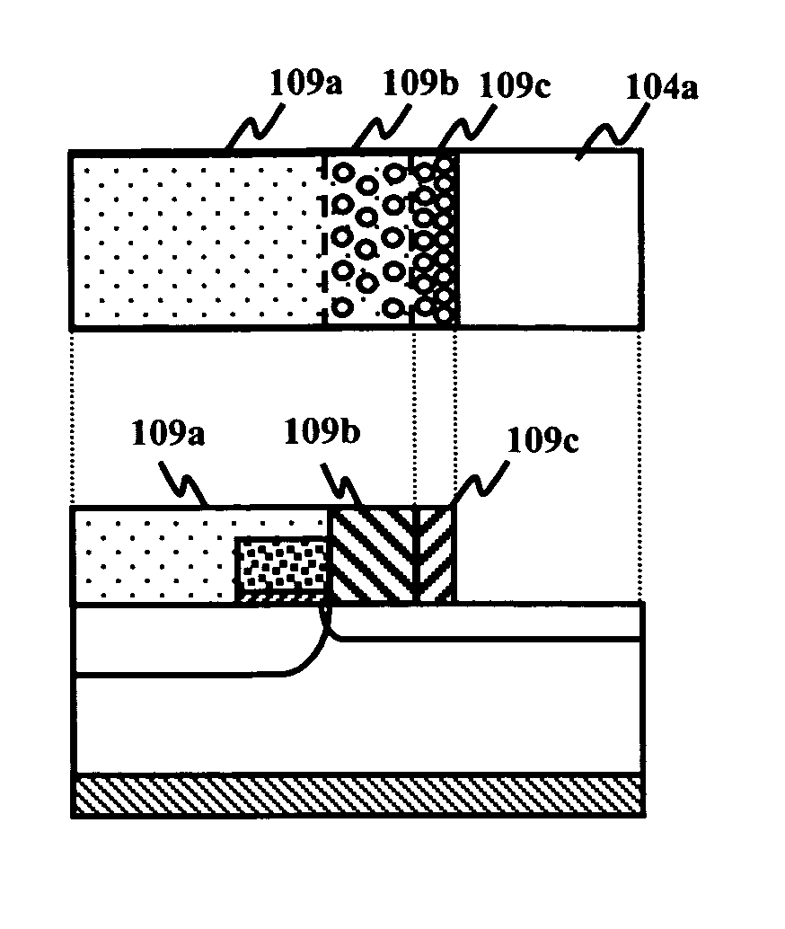
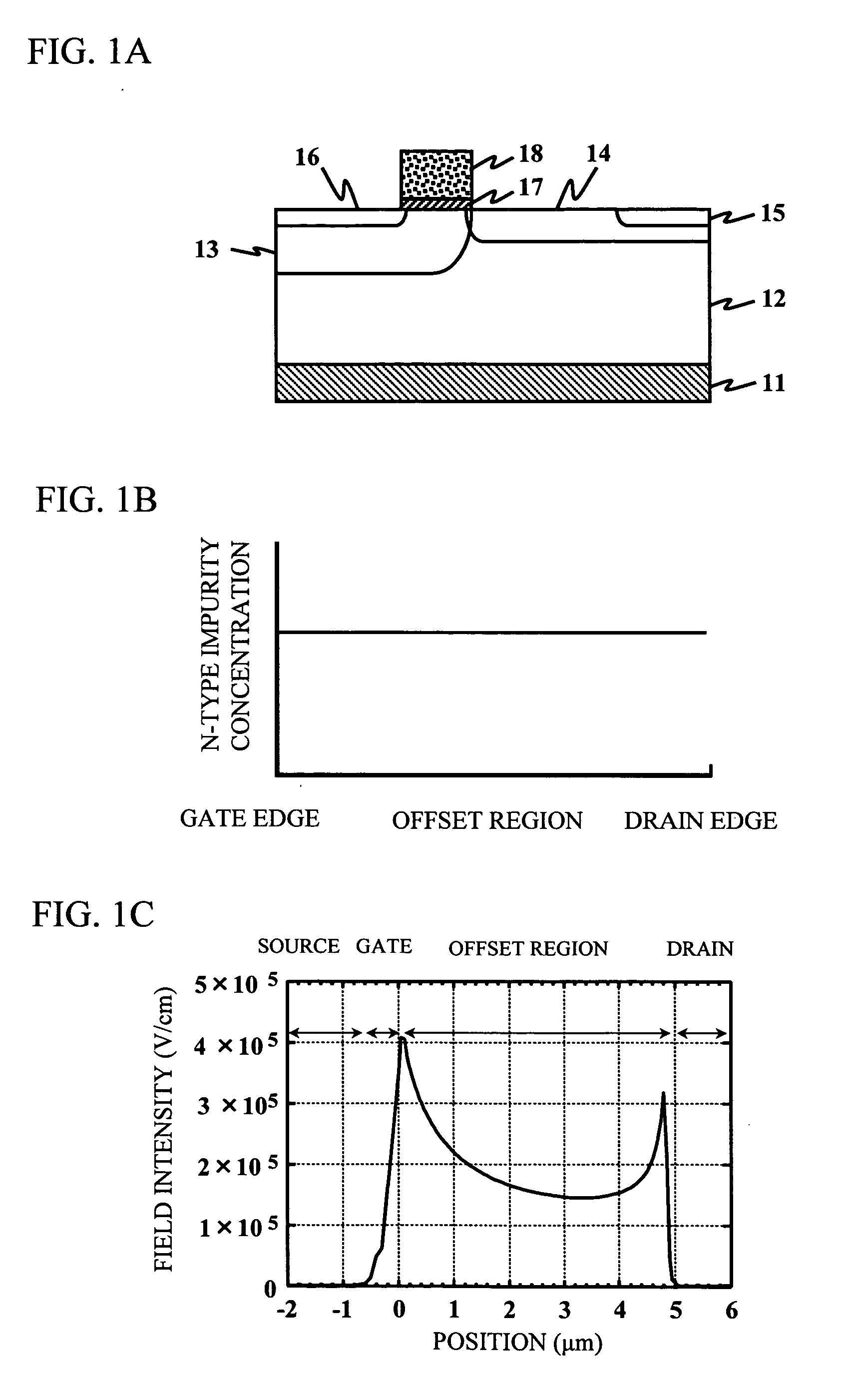
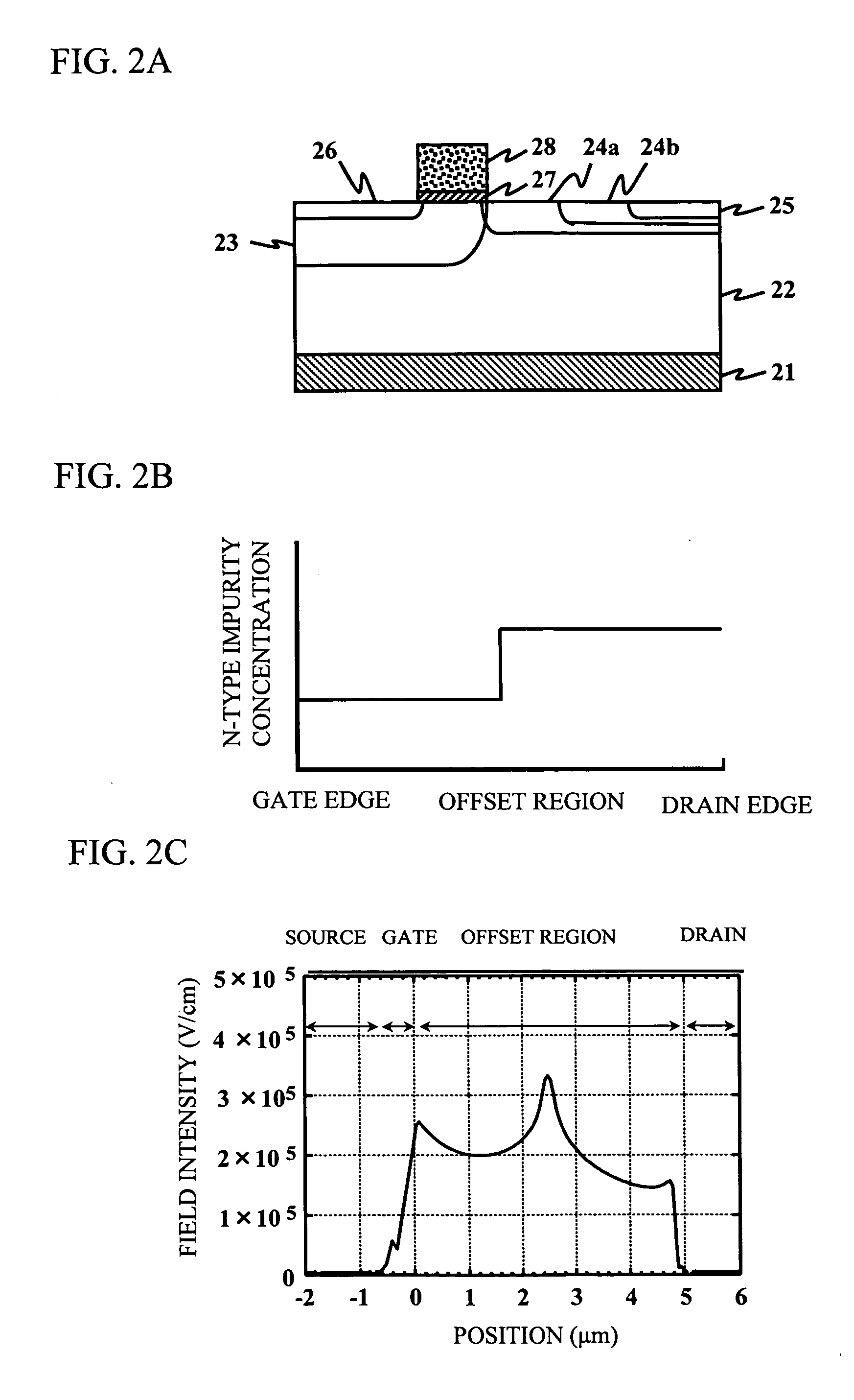
[0051]FIG. 4A is a schematic cross-sectional view of a LDMOS transistor in accordance with the present invention. Referring to FIG. 4A, the LDMOS transistor includes a heavily doped (P++) p-type substrate 101, a p-type epitaxial layer 102, which is epitaxially grown on a main surface of the substrate 101. The LDMOS transistor also includes a gate oxide film 107 and a gate electrode 108. A channel region 103 (P), an offset region 104 (N), a drain region 105 (N++), and a source region 106 (N++) are provided in a surface region of the p-type epitaxial layer 102. The offset region 104 includes three regions having different impurity concentrations, namely, a first offset region 104a, a second offset region 104b, and a third offset region 104c.
[0052]FIG. 4B shows a profile of an n-type impurity concentration in the offset region of the LDMOS transistor shown in FIG. 4A. The first offset region 104a extending from the edge of the gate and the third offset region 104c extending from the d...
second embodiment
[0069] A description will be given of a second embodiment of the present invention. The second embodiment of the present invention intends to reduce the electric field intensities at the edge of the gate and the edge of the drain in the semiconductor device having a field plate electrode provided above a semiconductor substrate.
[0070]FIG. 9A is a schematic cross-sectional view of an offset-type gate LDMOS transistor 100 having a field plate electrode 110. The field plate electrode 110 is set at a ground potential, and is located in the offset region 104 to reduce the electric field intensity thereof.
[0071]FIG. 9B shows distribution of the electric field intensity in the offset region 104 of the LDMOS transistor shown in FIG. 9A. For comparison, FIG. 9C shows the electric field intensity distribution in the offset region without the field plate electrode. As is obvious from FIGS. 9B and 9C, the electric field intensity distribution in the offset region 104 can be changed by providi...
third embodiment
[0076] A description will be given of a third embodiment of the present invention. FIG. 12 is a schematic cross-sectional view of the LDMOS in accordance with the third embodiment of the present invention. The semiconductor device is configured to include the impurity distribution in the offset region in accordance with the first embodiment of the present invention and the impurity distribution at the drain edge in accordance with the second embodiment of the present invention.
[0077] The semiconductor device in accordance with the third embodiment of the present invention may be fabricated by the same process as that of the first embodiment of the present invention. So, the description is omitted here. It is possible to obtain the higher breakdown voltage of the semiconductor device so that the energy band does not change drastically in the offset region. In addition, it is possible to suppress the degradation of the device characteristics due to injection of hot electrons by reduc...
PUM
 Abstract
Description
Claims
Application Information
 - Generate Ideas
- Intellectual Property
- Life Sciences
- Materials
- Tech Scout
- Unparalleled Data Quality
- Higher Quality Content
- 60% Fewer Hallucinations
Browse by: Latest US Patents, China's latest patents, Technical Efficacy Thesaurus, Application Domain, Technology Topic, Popular Technical Reports.
© 2025 PatSnap. All rights reserved.Legal|Privacy policy|Modern Slavery Act Transparency Statement|Sitemap|About US| Contact US: help@patsnap.com