Emitter structure with a protected gate electrode for an electron-emitting device

a gate electrode and electron-emitting device technology, which is applied in the manufacture of electrode systems, electric discharge tubes/lamps, and discharge tubes luminescent screens, etc., can solve the problems of high redundant electron sources for display, critical problems such as electrical arcing, and inability to fully prevent arcing, so as to achieve higher etch selectivity

Inactive Publication Date: 2005-10-27
ARROW CAPITAL +1
View PDF21 Cites 29 Cited by
  • Summary
  • Abstract
  • Description
  • Claims
  • Application Information

AI Technical Summary

Benefits of technology

[0012] To address this arcing problem, a cathode structure for an electron-emitting device includes a passivation layer, or other dielectric or insulating material, situated over or otherwise protecting the gate layer. To minimize exposure of the gate electrode to the anode while allowing exposure of the gate electrode for providing an electric field for drawing electrons from the emitter, the passivation layer covers and overhangs the gate layer on a top side thereof. This leaves an underside or other portion of the gate electrode exposed to the emitter structure while still protected from the anode structure. The passivation layer covers the gate electrode at least in part to inhibit arcing between the gate electrode and the anode structure.
[0014] In another embodiment, a method for making a cathode structure having an overhanging passivation layer comprises forming an emitter electrode on a substrate, forming an insulating layer over the emitter electrode, forming a gate electrode over the insulating layer, forming a passivation layer over the gate electrode, and forming at least one emitter hole through the insulating layer and the passivation layer (and possibly through the gate electrode). The passivation layer is formed so that it overhangs the gate electrode over the emitter hole or otherwise protects the gate electrode from arcing with an anode placed opposite the cathode structure. In one embodiment, where the emitter hole is formed by etching, the passivation layer and the insulating layer are selected so that the passivation layer has a higher etch selectivity relative to the insulating layer.

Problems solved by technology

This provides a highly redundant electron source for the display.
A problem arises in the design of such displays, however, due to their use of electric fields between the emitters and the other electrodes to cause emission of the electrons for driving the display.
In vacuum electronics, electrical arcing can be a critical problem for the proper operation of field emission electron-emitting devices.
As described, the arcing problem is related to the varying potentials of the cathode, faceplate, and spacer materials and structures, and specifically to the two electrodes that are commonly found therebetween—the gate electrode of the cathode and the anode electrode of the faceplate.
But these solutions have left portions of the gate layer exposed and have therefore not fully prevented arcing between the gate electrode and anode.

Method used


Image

  • Emitter structure with a protected gate electrode for an electron-emitting device
  • Emitter structure with a protected gate electrode for an electron-emitting device
  • Emitter structure with a protected gate electrode for an electron-emitting device

Examples


Embodiment Construction

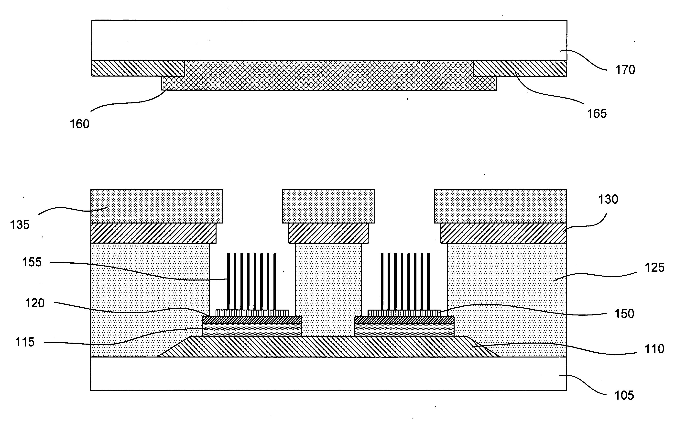
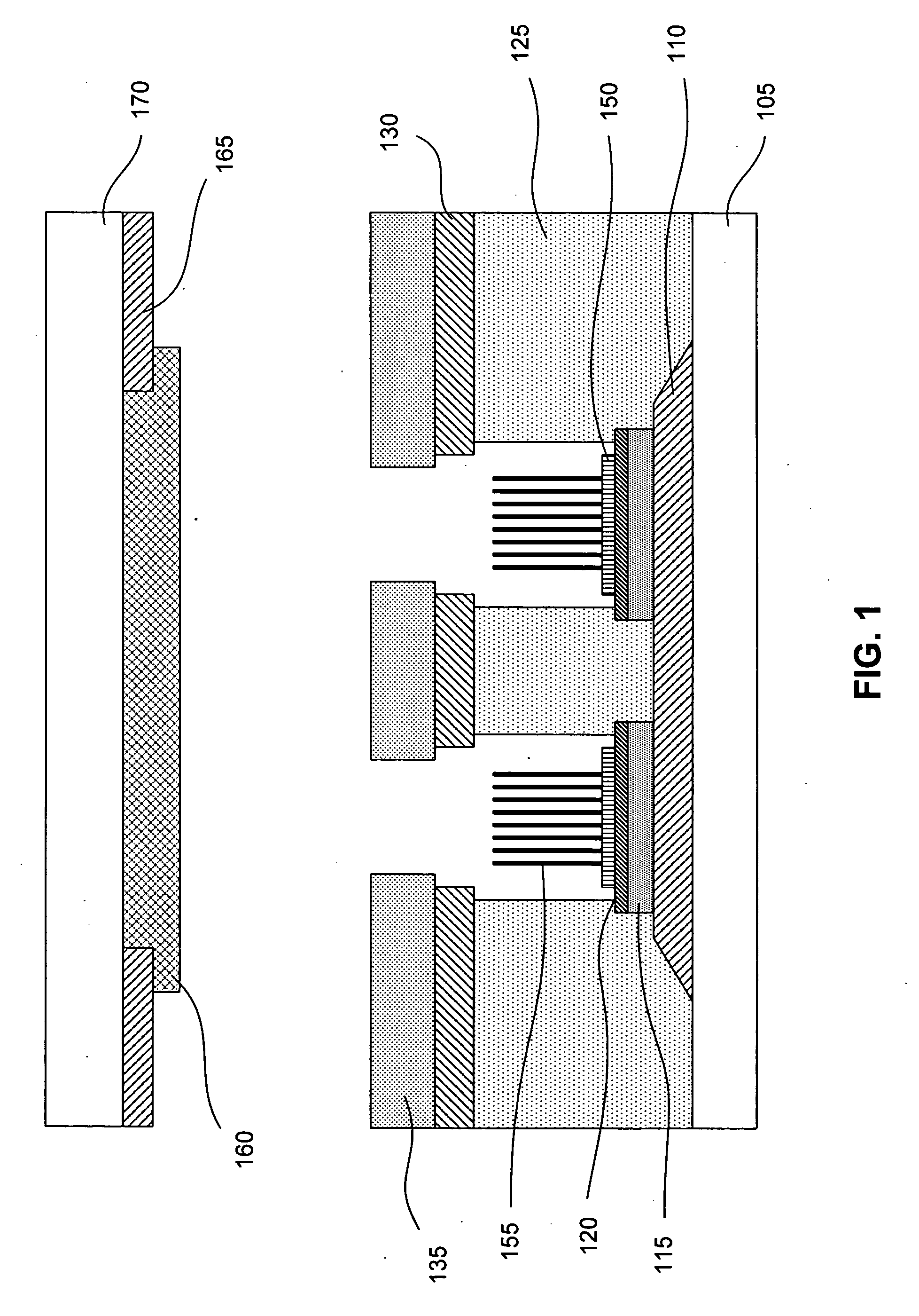
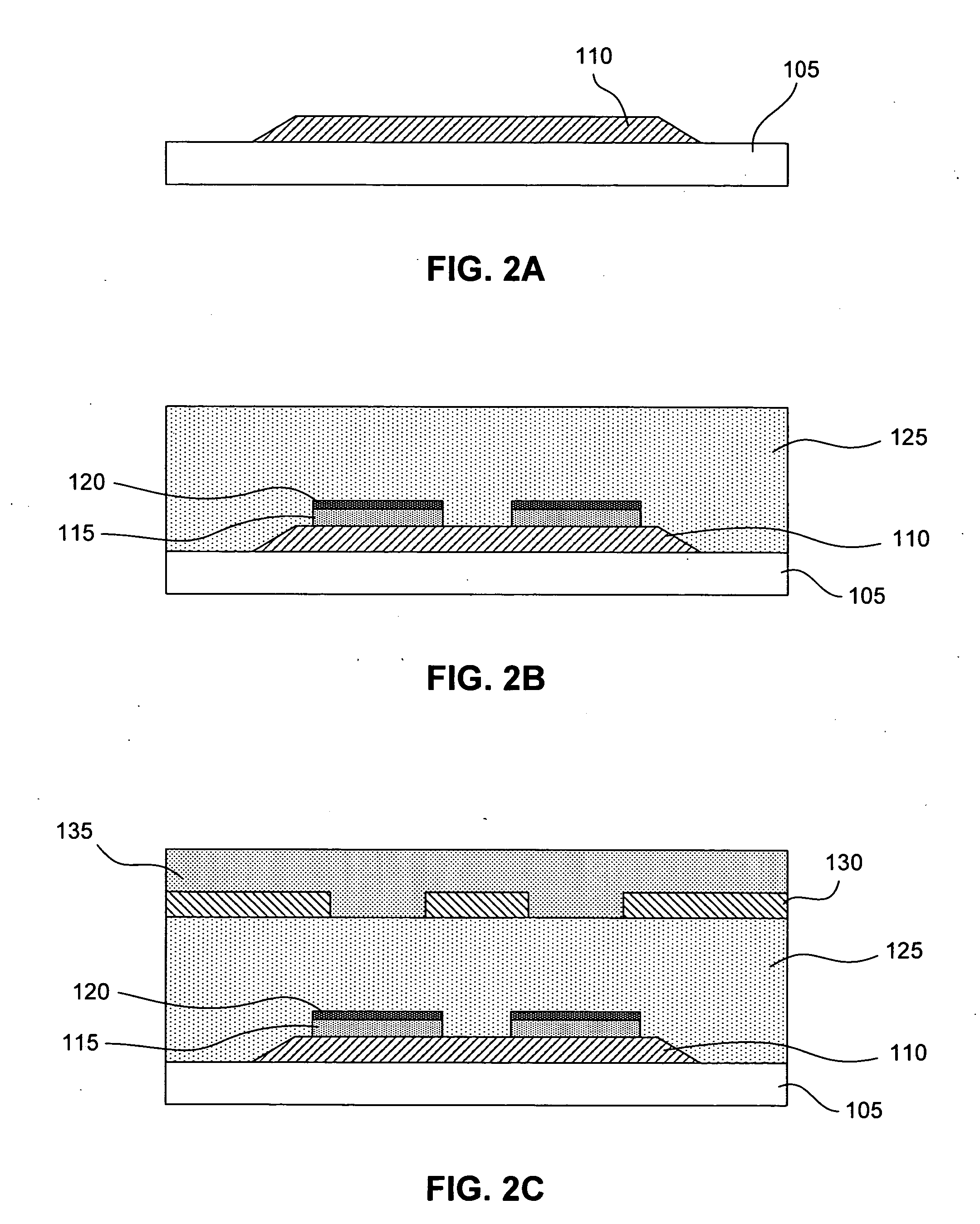
[0018]FIG. 1 illustrates one embodiment of a field emission device for emitting electrons, such as a portion of a CNT-based field emission display described above. The field emission device shown in FIG. 1 comprises two main structures: a cathode structure and an anode structure. The cathode structure includes a number of layers of material deposited over a substrate 105, such as glass. In one embodiment, the layers of the cathode structure include an emitter electrode 110, a resistor layer 115, a barrier layer 120, an insulating (or dielectric) layer 125, a gate electrode 130, and a passivation layer 135. The cathode structure further comprises electron emitters 155, such as carbon nanotubes, which are situated in one or more emitter holes formed through a portion of the cathode structure. Preferably, the electron emitters 155 are disposed on or in electrical coupling with the emitter electrode 110. The electron emitters may be formed from a catalyst layer 150, which rests over the...


PUM


Abstract

A cathode structure of a field emission device includes a gate electrode that is protected by a passivation layer. In one method for manufacturing such a field emission device, an emitter hole is formed through an insulating layer such that the passivation layer overhangs the gate layer, which overhangs an insulating layer. When used in a display system, the gate layer is exposed to an emitter electrode but shielded from an anode.

Description

CROSS REFERENCE TO RELATED APPLICATIONS [0001] This application claims the benefit of U.S. Provisional Application No. 60 / 563,075, filed Apr. 15, 2004, which is incorporated by reference in its entirety.BACKGROUND [0002] 1. Field of the Invention [0003] This invention relates generally to field emission devices, and in particular to cathode structures for field emission devices having protected gate electrodes. [0004] 2. Background of the Invention [0005] Flat panel displays (FPDs) using carbon nanotube (CNT) technology are replacing and superseding existing display technologies, including those that use cathode ray tubes (CRTs), thin film transistor liquid crystals (TFT-LCDs), plasma display panels (PDPs), and organic light emitting diodes (OLEDs). The emerging CNT-based flat panel display technology uses a process for generating pictures similar to the method used in CRTs. But instead of a CRT's single hot filament electron gun, CNT-based displays use a planar array of carbon nano...

Claims


Application Information

Patent Timeline
Patent Type & Authority Applications(United States)
IPC IPC(8): H01J1/02H01J1/62H01J3/02H01J9/02H01J29/06H01J63/04
CPCB82Y10/00H01J3/022H01J2329/00H01J29/06H01J2201/30469H01J9/025
Inventor KANG, SUNG GUBAE, WOO KYUNGSON, JONG WOOCHANG, CHUL HAKIM, JUNG JAE
Owner ARROW CAPITAL
Why Eureka
Try Eureka