High coherent power, two-dimensional surface-emitting semiconductor diode array laser

a semiconductor diode array, two-dimensional technology, applied in the direction of semiconductor laser structure details, semiconductor lasers, optical resonator shape and construction, etc., can solve the problems of high radiation loss, and low yield of in-phase-mode operating devices, so as to improve the sensitivity of laser-absorption spectroscopy, the effect of high efficiency

Active Publication Date: 2005-10-27
WISCONSIN ALUMNI RES FOUND
View PDF40 Cites 28 Cited by
  • Summary
  • Abstract
  • Description
  • Claims
  • Application Information

AI Technical Summary

Benefits of technology

[0014] The antiguided array structures of the present invention for the lateral dimension preferably have large index steps (e.g., Δn≈0.10), which ensure optical-mode stability against carrier and thermal induced dielectric-constant variations. The 2-D devices of the present invention combine antiguided phase locked arrays with surface emission from 2nd-order DFB / DBR grating structures. Unlike prior 2-D 2nd order grating DFB / DBR surface emitters, the present invention may utilize grating phase shifts around 180°, via a discrete central phase shift or a phase shift distributed along the length of the grating (e.g., a chirped grating), or a π-phase shifting surface film, to provide emission in a single lobe beam at no penalty in device efficiency. The grating structure, beside ensuring single longitudinal-mode operation, can be formed to act as a highly efficient selector of a single lateral mode, the in phase array mode. As a consequence, large aperture (e.g., 200 μm×1200 μm to 400 μm×1 cm) coherent laser diode sources in accordance with the invention have nearly uniform 2-D guided-field profiles and thus are able to operate in a stable, single diffraction-limited beam to watt-range CW output powers. Beam circularization can then be readily obtained utilizing commercially available optical components.
[0015] The present invention enables CW watt-range, stable, single mode laser light sources that may be utilized for applications such as room-temperature CW mid-IR (λ=3-5 μm) coherent light generation (via frequency up-conversion) that can provide several orders of magnitude increases in the sensitivity of laser-absorption spectroscopy for a wide array of non-invasive medical diagnostics (e.g., breath analysis), and for IR countermeasures; for the generation of hundreds of mWs of blue light via harmonic conversion for applications such as in biotechnology (e.g., flow cytometry) and for laser projection systems; for high-power low-noise, high-fidelity RF optical links; and for coherent free-space optical communications. The devices of the present invention are single frequency and thus ideally suited for scalability at the wafer level (via resonant leaky-wave coupling) to 20 units or more. This enables all-monolithic laser light sources capable of providing tens of watts of coherent, uniphase power for various applications, such as high-efficiency, high resolution magnetic resonance imaging with noble gases.
[0016] The surface-emitting devices of the present invention have the advantages over edge-emitting devices for the generation of high (greater than 1 W) CW coherent powers that: complete passivation of the emitting area is not needed for reliable operation, scalability at the wafer level becomes possible, and packaging is significantly simplified.
[0017] The semiconductor diodes of the present invention preferably utilize gain in the low-index lattice sites, which in turn allows long range coherent coupling via traveling waves. An effective π phase shift may be implemented to provide single-lobe operation. For example, the use of a π phase shifter centrally located in a second order grating serves to provide single-lobe, orthonormal beam emission with high efficiency (greater than 60%), and the use of gratings with dual spatial-mode selectivity provides both conventional longitudinal-mode selection and strong lateral-mode selection for phase-locked antiguided arrays. A grating with a continuously varying phase shift along the length of the grating may also be utilized to achieve single lobe operation. In the lateral direction, spatial coherence is obtained by using a phase-locked antiguided array, which corresponds to a 1-dimensional active photonic lattice, and using traveling waves for element coupling. The coupling is resonant and long-range by having the high-index regions correspond to an integral number of lateral half waves, thus making the structure fully transmissive. Although the index step may be relatively small compared to those commonly used in photonic lattices, photonic bands and band gaps are formed. Such devices are in effect lateral 2nd-order complex coupled DFB structures whose 2nd diffraction order provides lateral coupling while the 1st diffraction order provides propagation in a direction parallel to the array elements and edge emission for edge emitting devices. At lateral resonances, the second order Bragg condition is exactly satisfied, and the stopgaps disappear, i.e., at resonance, full transmission across the photonic lattice is allowed, effectively making such devices photonic band pass devices. At resonance, antiguided arrays become pure gain-coupled DFBs, which are well known to have no stopgaps and thus will lase at the Bragg frequency. Strong light absorption in the interelement regions provides discrimination of modes with significant interelement field, thus favoring the in-phase mode.
[0018] In the longitudinal direction, coherence is obtained by using a 2nd-order grating with a DFB region for gain, partial feedback and outcoupling, and DBR regions for strong frequency-selective feedback and partial outcoupling, effectively providing a second order photonic band gap structure with light outcoupling. Unlike microcavity PBG structures with built-in lattice defect (defect lasers), the photonic band gap structure in the present invention does not have lattice defects, thus allowing for full transmission of light over large distances and thus permitting the generation and surface emission of high coherent power from large apertures. Thus, the present invention combines 2nd-order photonic lattices in both the lateral (PBP structure) and the longitudinal (PBG structure) directions. The two lattices are interconnected in that the longitudinally-placed gratings act as a highly effective selector of the desired traveling-wave mode in the lateral direction—the in-phase array mode.

Problems solved by technology

Although in a single antiguide the radiation losses can be quite high, closely spacing antiguides in linear arrays significantly reduces the device losses, since radiation leakage from individual elements mainly serves the purpose of coupling the array elements.
However, ROW arrays can be prone to self-pulsations either if saturable absorption occurs in lossy interelement regions or when imaging, in intracavity Talbot-type spatial filters, is disturbed by GSHB.
Single-frequency pulsed operation can be achieved for edge-emitting devices by using DFB gratings, but the yield of in-phase-mode operating devices has been quite low, since the effective yield is a strong function of the grating phase(s) with respect to the cleaved mirror facet(s).
Furthermore, the guided-field pattern is highly nonuniform, making the device vulnerable to multimoding via longitudinal GSHB. C. H. Henry, et al., “Observation of Destructive Interference in the Radiation Loss of Second-Order Distributed Feedback Lasers,” IEEE J. QE, Vol. 21, 1985, pp.
However, preferential carrier injection is not a long-term reliable approach, and the scheme, due to the necessity for weak coupling grating, inherently leads to inefficient devices (about 10% efficiency).
The metal-grating variant of the approach is feasible but introduces too much of a penalty loss for the symmetric mode, such that efficiencies are at best 25-30%, and the gain thresholds are quite high (about 70 cm−1).
However, current e-beam lithography allows writing of gratings only 400-600 μm long, and for devices requiring relatively long gratings (e.g., about 1,500 μm), fabrication by e-beam lithography is not advisable.
However, none of these devices have a built-in dielectric structure for lateral-optical-mode control and stability, and as a result are vulnerable to temperature and carrier induced dielectric-constant variations.
An example of such behavior is the unstable resonator device which, while operating single-mode to high peak pulsed power in a single off-normal beam, readily becomes multimode in CW operation due to thermal lensing.

Method used


Image

  • High coherent power, two-dimensional surface-emitting semiconductor diode array laser
  • High coherent power, two-dimensional surface-emitting semiconductor diode array laser
  • High coherent power, two-dimensional surface-emitting semiconductor diode array laser

Examples


Embodiment Construction

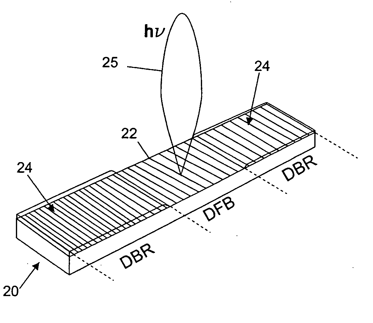
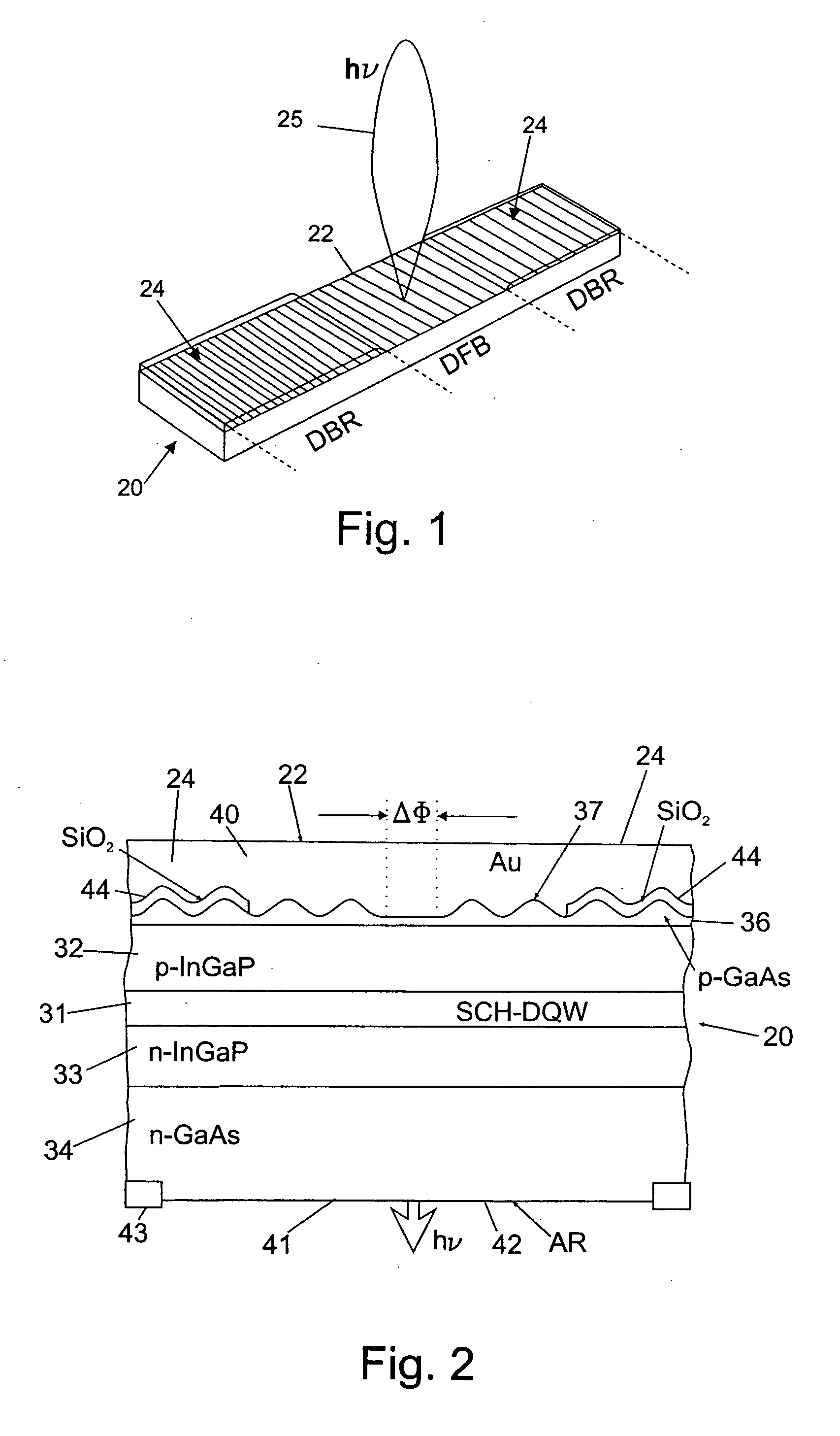
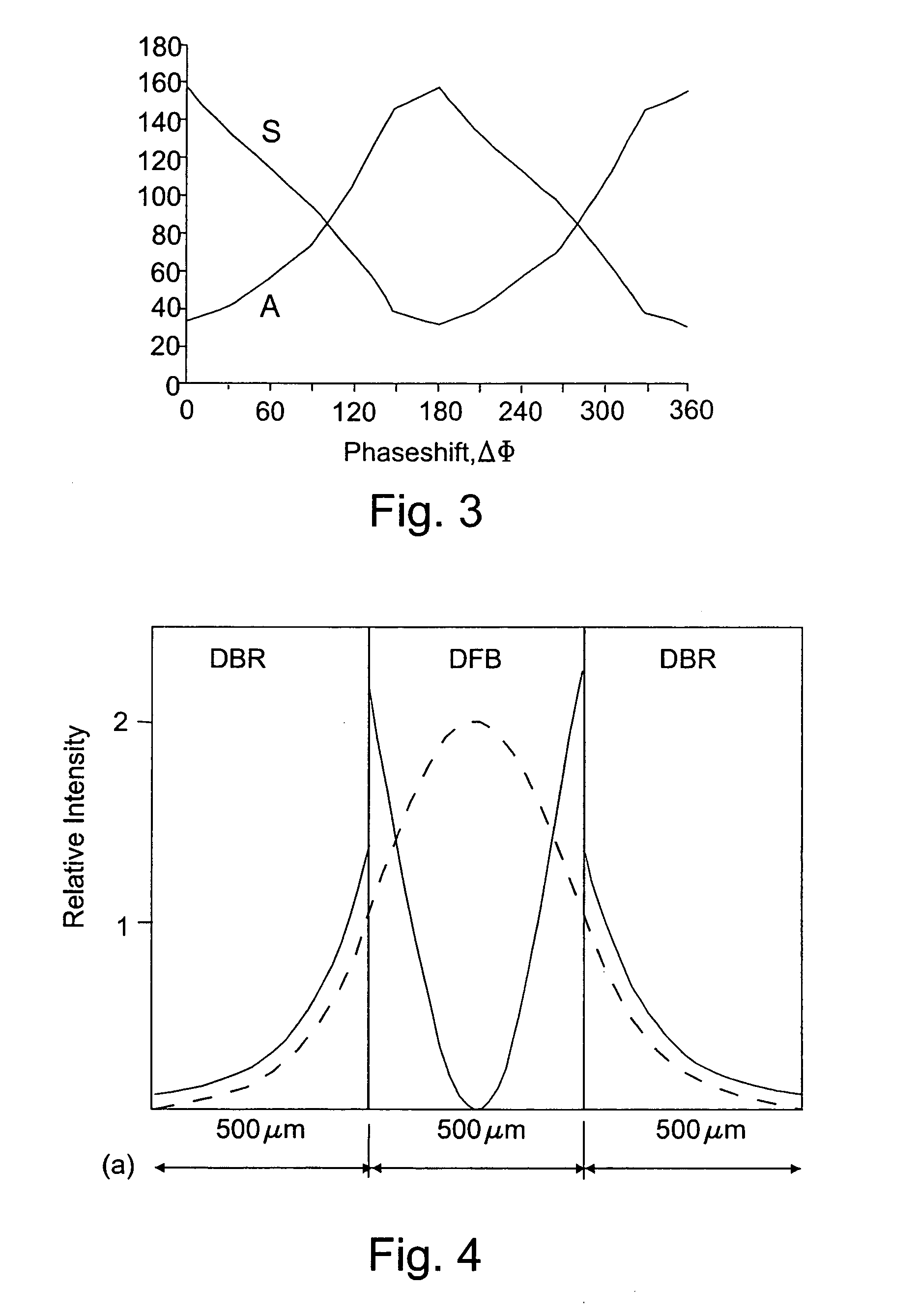
[0045] For purposes of illustrating the invention, a single surface-emitting DFB / DBR device element that may be utilized in the laser diode array of the invention is shown generally at 20 in FIG. 1. This type of device includes a distributed feedback (DFB) grating structure 22 bounded longitudinally by two distributed Bragg reflectors (DBRs) 24. Operation in a single orthonormal beam (illustrated at 25) can be attained utilizing at or near a half-wave (7c) central grating phase shift in the DFB grating 22. A particular embodiment of a semiconductor laser structure of this type is shown for exemplification in FIG. 2, although it is understood that other devices of this type may also be utilized, as described, for example, in published International Application WO 01 / 13480 and U.S. Pat. No. 6,810,053. As discussed further below, single beam operation can also be obtained utilizing a grating with a distributed phase shift or a π-phase shift film on the output surface of a device whose ...


PUM


Abstract

A semiconductor laser is formed on a semiconductor substrate with an array of laterally spaced laser device elements each including a second order distributed feedback grating bounded by distributed Bragg reflector gratings. The device elements in which the distributed feedback grating and the distributed Bragg reflector gratings are formed have a lower effective index than the index of the interelement regions and are spaced so as to form an antiguided array.

Description

CROSS-REFERENCE TO RELATED APPLICATIONS [0001] This application is a continuation-in-part of and claims priority to U.S. patent application Ser. No.10 / 345,613, filed on Jan. 16, 2003, pending, which claims the benefit of provisional application No. 60 / 350,826, filed Jan. 18, 2002, the disclosures of which are incorporated by reference.STATEMENT OF GOVERNMENT RIGHTS FIELD OF THE INVENTION [0002] This invention pertains generally to the field of semiconductor diode lasers and diode laser arrays. BACKGROUND OF THE INVENTION [0003] Phase locked arrays of antiguide laser structures were demonstrated over a decade ago. See, D. Botez, et al. “High-Power Diffraction Limited Beam Operation from Phase Locked Diode Laser Arrays of Closely Spaced ‘Leaky’ Wave Guides (Antiguides),” Appl. Phys. Lett., Vol. 53, 1988, pp. 464 et seq. In an antiguide laser, the antiguide core has an index no lower than the cladding index, n1. Whereas in a positive index guide, light is trapped in the guide core via ...

Claims


Application Information

Patent Timeline
Patent Type & Authority Applications(United States)
IPC IPC(8): H01S3/00H01S3/08H01S5/00H01S5/02H01S5/12H01S5/125H01S5/18H01S5/343H01S5/40H01S5/42
CPCB82Y20/00H01S5/0014H01S5/028H01S5/1032H01S5/1203H01S5/205H01S5/125H01S5/187H01S5/34313H01S5/4081H01S5/42H01S5/124
Inventor BOTEZ, DAN
Owner WISCONSIN ALUMNI RES FOUND
Why Eureka
Try Eureka