Organic semiconductor element, production mehtod therefor and organic semiconductor device

a technology of organic semiconductors and semiconductor elements, which is applied in the direction of solid-state devices, transistors, thermoelectric devices, etc., can solve the problems of difficult to make the surface area of a substrate larger, difficult to achieve expected characteristics, and difficult to make the conduction between. achieve the effect of low surface energy

Inactive Publication Date: 2005-11-10
CANON KK
View PDF9 Cites 35 Cited by
  • Summary
  • Abstract
  • Description
  • Claims
  • Application Information

AI Technical Summary

Benefits of technology

[0018] More specifically, a first invention of the present invention is an organic semiconductor element comprising a gate electrode, a gate insulating layer, an organic semiconductor layer, source/drain electrodes and a protective film...

Problems solved by technology

In this case, the PTFE film is formed on the substrate surface by sliding a solid lump of PTFE under a certain pressure so that it is difficult to make the area of a substrate larger.
Additionally, the molecules in the organic semiconductor layer are aligned uniformly along the orientation direction of the PTFE film so that the carrier conduction between the molecules becomes difficult to occur, and accordingly the expected characteristics are hardly obtained.
In this case, the intermolecular conduction is also difficult to occur on the above-de...

Method used


Image

  • Organic semiconductor element, production mehtod therefor and organic semiconductor device
  • Organic semiconductor element, production mehtod therefor and organic semiconductor device
  • Organic semiconductor element, production mehtod therefor and organic semiconductor device

Examples


example 1

[0098] In the first place, description is made on the substrate used in the organic semiconductor device according to the present Example and the cleaning method.

[0099] The silicon substrate used in the present Example was a p-type substrate doped with boron. The resistivity of the substrate was 0.1 to 0.2 Ωcm. The crystal axis was .

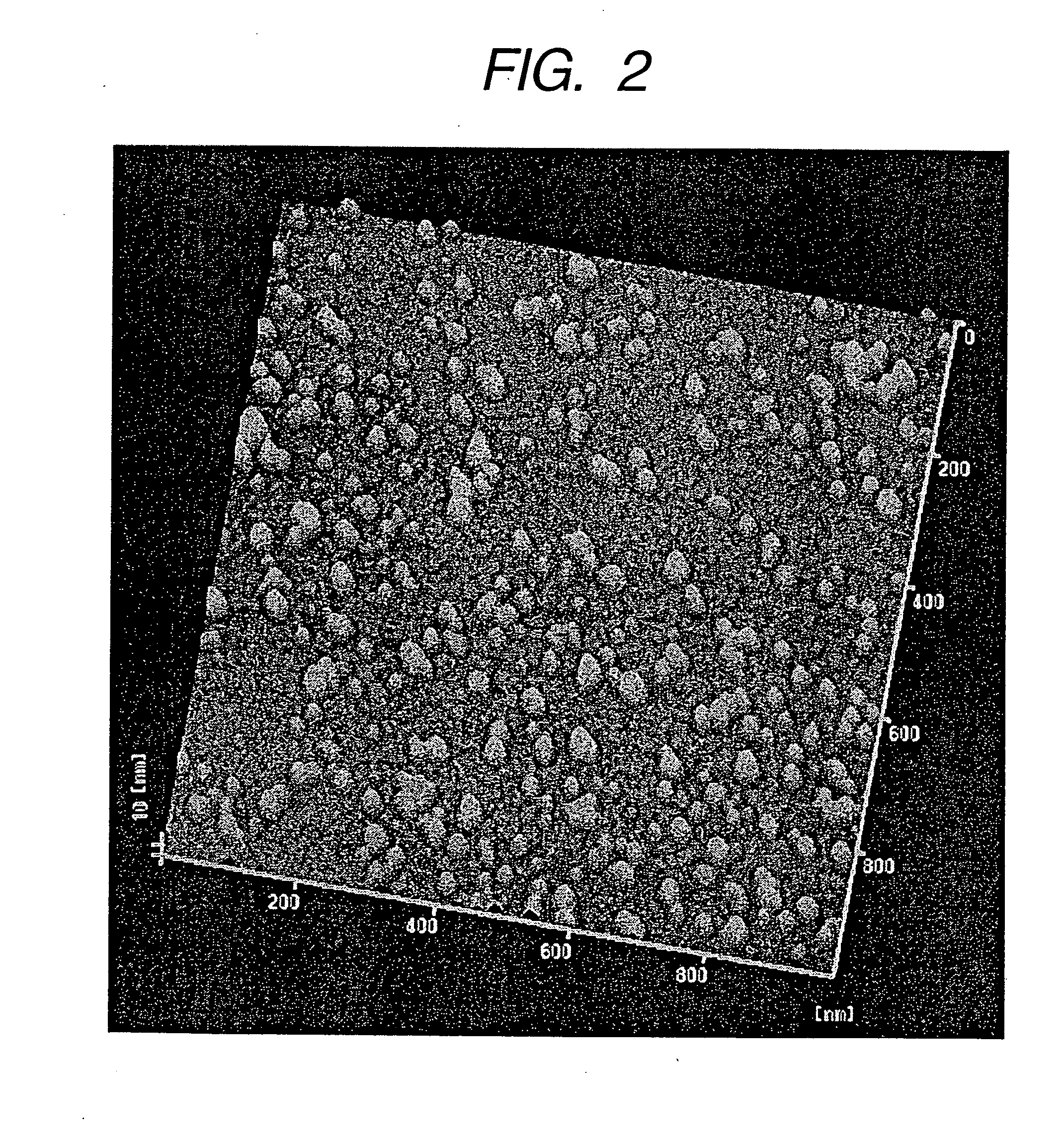
[0100] A SiO2 film was formed on the silicon substrate. The SiO2 film was 200 nm in film thickness, which was formed on the surface of the silicon substrate by the wet thermal oxidation method. The oxidation conditions were the furnace temperature set at 95° C. and the inflow ratio of H2 and O2 set at 0.5.

[0101] The cleaning method of the silicon substrate was as follows. Twice repeated was the process in which silicon substrate was soaked in acetone with a purity of 99% or higher and subjected to ultrasonic cleaning for 5 min and then the substrate was soaked in purified water and subjected to ultrasonic cleaning for 5 min. After the cleaning, purifi...

example 2

[0141] Description is made below on the embodiment in which the organic semiconductor element according to the present invention was utilized in an active matrix liquid crystal display device, with reference to FIGS. 10 through 12C.

[0142]FIG. 10 shows the active matrix liquid crystal display device according to the present invention.

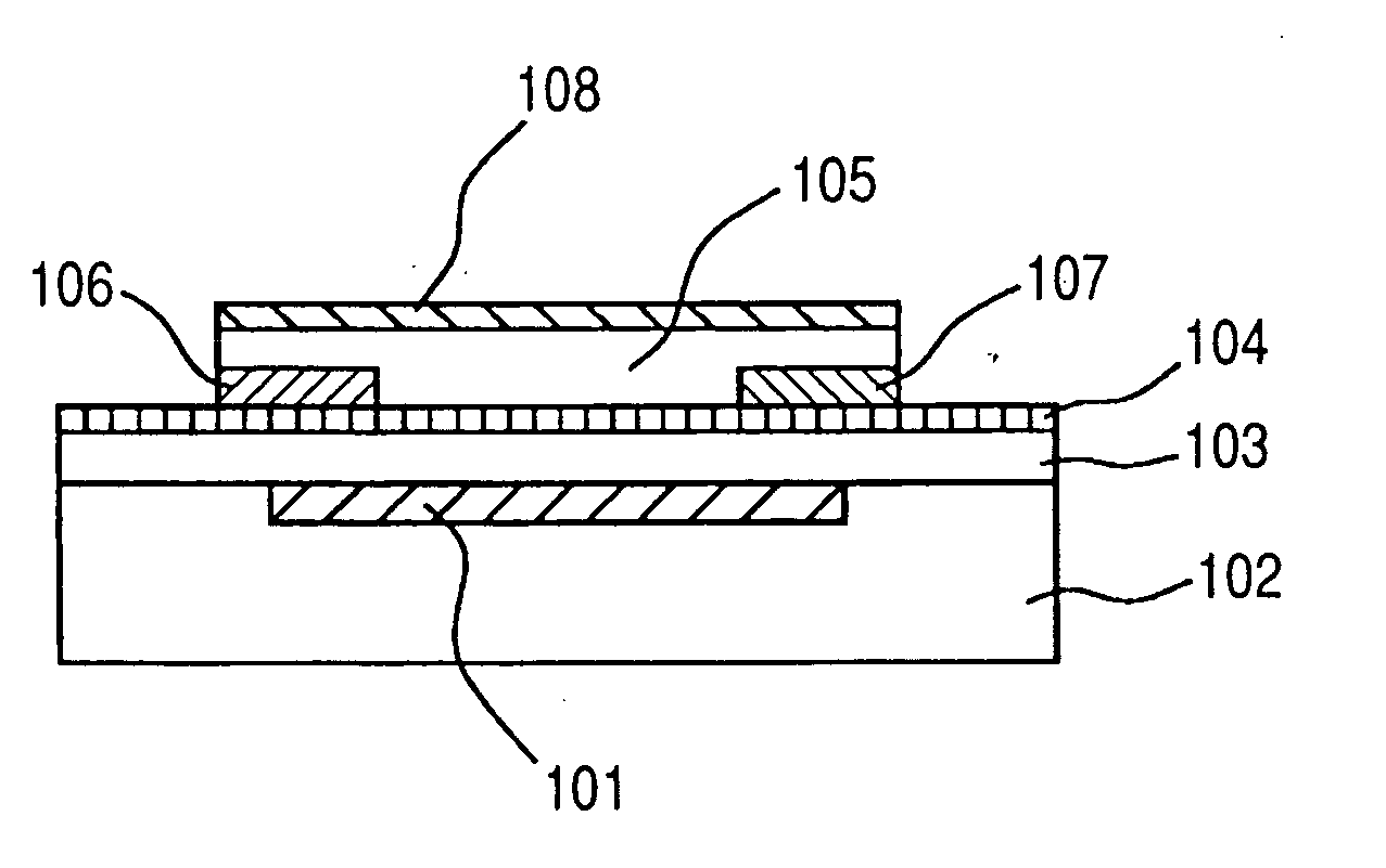
[0143]FIG. 11 shows a sectional view of the active matrix liquid crystal display device taken along the line 11-11 of FIG. 10. Reference numeral 401 denotes a glass substrate, 402 a gate electrode, 403 a gate insulating film, 404 an island-shaped protrusion layer on which island-shaped protrusions with a low surface energy are scattered, 405 a source electrode, 406 a drain electrode, 407 a pentacene vapor-deposited film, 408 and 408′ signal wires, 409 and 409′ scanning wires, 410 a pixel electrode, 411 a SiNx protective film, 413 and 413′ oriented films, 414 an opposed electrode, 415 a liquid crystal composition, 416 a gap, 417 a spacer bead, 418 and 4...

example 3

[0149] Description is made on a production method of the IC information tag.

[0150] As for the explanation of FIG. 13, FIG. 13 shows a portion of an IC substrate. For simplicity of FIG. 13, only one inverted TFT is shown, but this one device is a large integrated array device. Additionally, the elements and the like shown in the figure are not accurately scaled. The IC information tag in the present Example has a structure in which an organic semiconductor is arranged on the downside, and a dielectric memory is stacked thereover. In the present invention, an organic dielectric memory is used, and two transistors are used to operate the memory. If the degree of integration is not taken into account, an inorganic dielectric can be combined in one and the same plane. A structure is also possible in which one dielectric is allotted to one transistor. Additionally, an organic transistor may be formed on an organic dielectric memory, in a reversed manner.

[0151]FIG. 14 is a schematic diag...


PUM


Abstract

An organic semiconductor element is provided which has the controlled crystalline state of a vapor-deposited pentacene layer and a high mobility with low voltage driving. The organic semiconductor element is formed by providing a gate electrode 101 on the surface of a substrate 102, providing thereon a gate insulating layer 103, providing on the surface of the gate 102 insulating layer 103 an island-shaped protrusion layer 104 having dispersed and island-shaped protrusions with a low surface energy, providing on the island-shaped protrusion layer 104 a source electrode 106 and a drain electrode 107 with a distance therebetween, providing thereon an organic semiconductor layer 105 in contact with the island-shaped protrusion layer 104 and both electrodes 106 and 107, and further providing a protective film 108 on the organic semiconductor layer 105.

Description

TECHNICAL FIELD [0001] The present invention relates to an organic semiconductor element, the production method therefor, an active matrix type display device that utilizes the organic semiconductor element, and an organic semiconductor device that utilizes the organic semiconductor as an IC-card electronic tag. BACKGROUND ART [0002] Over the past decade, IC technology for use of an organic semicondutctor thin film transistor (organic TFT) has been proposed. The main attractive points of such circuitry come from the expectations for easy processing and adaptability to a flexible substrate. These advantages are expected to be utilized in the low cost IC technology to be appropriately applied to smart cards, electronic tags, displays and the like. [0003] A general organic TFT is composed of a glass substrate, a gate electrode, a gate insulating film, a source electrode, a drain electrode and an organic semiconductor film. Variation of a voltage applied to the gate electrode (gate volt...

Claims


Application Information

Patent Timeline
IPC IPC(8): H01L51/05H01L21/312H01L21/316H01L29/786H01L51/00H01L51/30H01L51/40
CPCH01L21/312H01L21/3127H01L21/31612H01L51/0003H01L51/107H01L51/0012H01L51/0055H01L51/0529H01L51/0545H01L51/001H10K71/164H10K71/191H10K71/12H10K85/623H10K10/474H10K10/88H10K10/466H01L21/0212H01L21/02164H01L21/02118
Inventor UNNO, AKIRA
Owner CANON KK
Why Eureka
Try Eureka