
Organic electroluminescent device using mixture of phosphorescent material as light-emitting substance

Inactive Publication Date: 2005-11-10
SAMSUNG DISPLAY CO LTD
View PDF19 Cites 2 Cited by
  • Summary
  • Abstract
  • Description
  • Claims
  • Application Information

AI Technical Summary

Benefits of technology

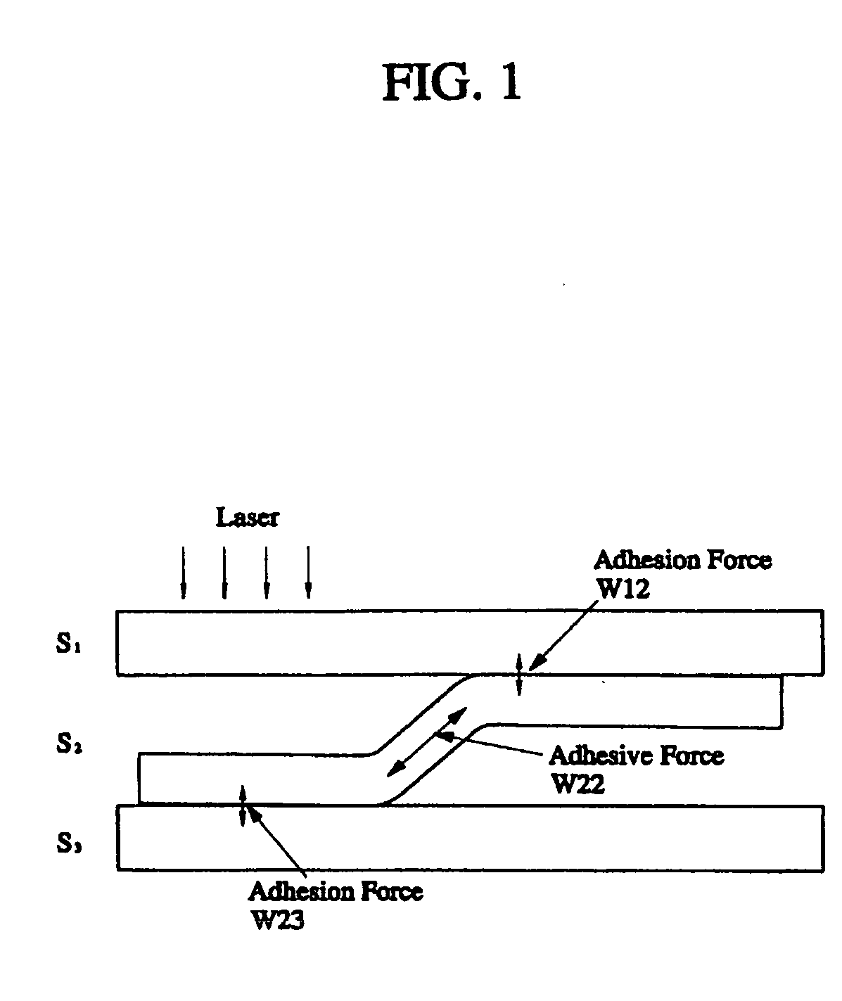
[0010] Accordingly, it is an aspect of the present invention to provide an organic EL device in which a high molecular light-emitting layer can be patterned, and color purity and light-emitting characteristics are improved when fabricating a full color organic polymer EL device by laser induced thermal imaging.

Problems solved by technology

A low molecular organic EL device is disadvantageous in terms of a mass-production since a full color device is fabricated by depositing each layer using a mask while a fluorescent device and a phosphorescent device are fabricated by introducing each layer using a vacuum-deposition.
However, devices using a phosphorescent material have not been reported regardless of their possibility since they are limited in the spin-coating process.

Method used


Image

  • Organic electroluminescent device using mixture of phosphorescent material as light-emitting substance
  • Organic electroluminescent device using mixture of phosphorescent material as light-emitting substance

Examples


examples

[0044] Examples provided below are for an illustrative purpose and to help understand the present invention. Therefore, it is understood that the present invention is not limited to the following examples.

examples 1 and 4

[0045] A method of fabricating an organic EL device using a light-emitting layer according to the present invention is as follows.

[0046] Poly(vinylcarbazole) (PVK: manufactured by SIGMA-ALDRICH CORPORATION) as a matrix of a host substance, and 4,4′-N,N′-dicarbazole-biphenyl (CBP; manufactured by UNIVERSAL DISPLAY CORPORATION), as a low molecular hole transporter material, were respectively dissolved into toluene in the range of 1.0 to 2.0 wt. %. An organic complex including iridium, that is, tris(2-phenylpyrridine)iridium(IrPPy; manufactured by UNIVERSAL DISPLAY CORPORATION) as a phosphorescent dopant, was dissolved into dichloroethane (DCE; manufactured by SIGMA-ALDRICH CORPORATION) in a concentration of 0.1 to 0.2%. Each of the materials was mixed in appropriate weight ratios after completely dissolving the solutions by sufficiently agitating each solution at a temperature of 60° C. for more than 3 hours.

[0047] A mixture film having a thickness of 30 to 50 nm was prepared by spi...

examples 5 to 8

[0048] Examples 5 to 8 have the same structures of devices as in Examples 1 to 4, except that oxadiazole based PBD was used as the low molecular hole transport material. Poly(vinylcarbazole) (PVK: manufactured by SIGMA-ALDRICH CORPORATION), as a matrix of host and 2-(4-biphenylyl)-5-(4-tert-butylphenyl)-1,3,4-oxadiazole (PBD; manufactured by SIGMA-ALDRICH CORPORATION), as the low molecular hole transport material, were respectively dissolved into toluene in the range of 1.0 to 2.0 wt. %. An organic complex including iridium, that is, tris(2-phenylpyrridine)iridium (IrPPy; manufactured by UNIVERSAL DISPLAY CORPORATION), as a phosphorescent material, was dissolved into dichloroethane (DCE; manufactured by SIGMA-ALDRICH CORPORATION) in a concentration of 0.1 to 0.2%. Each of the materials was mixed in appropriate weight ratios after completely dissolving the solutions by sufficiently agitating each solution at a temperature of 60° for more than 3 hours. A mixture film having a thicknes...


PUM

PropertyMeasurementUnit
Fractionaaaaaaaaaa
Fractionaaaaaaaaaa
Fractionaaaaaaaaaa

Abstract

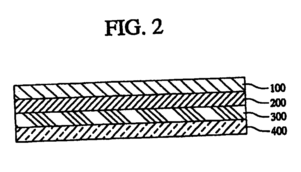
An organic EL device which includes a first electrode, a hole transport layer, a light-emitting layer, and the second electrode, wherein the light-emitting layer includes a mixed light-emitting film of a host substance, which is capable of transferring an energy to another light-emitting polymer by absorbing the energy, and a phosphorescent dopant which is capable of emitting light using a triplet state after absorbing the energy received. Accordingly, the light-emitting layer can be patterned, and a color purity and light-emitting characteristics of a full color organic polymer EL device, produced through a laser induced thermal imaging operating, can be improved.

Description

CROSS-REFERENCE TO RELATED APPLICATIONS [0001] This application claims the benefit of Korean Application No. 2002-34692, filed Jun. 20, 2002, in the Korean Intellectual Property Office and is a continuation in part of U.S. patent application Ser. No. 10 / 404,134, the disclosures of which are incorporated herein by reference. BACKGROUND OF THE INVENTION [0002] 1. Field of the Invention [0003] The present invention relates to an organic polymer electroluminescent device, and more particularly, to an organic polymer electroluminescent device using a mixture of laser induced thermal imaging enabling phosphorescent materials as a light-emitting substance. [0004] 2. Description of the Related Art [0005] Generally, an organic electroluminescent device includes an anode and a cathode, a hole injection layer, a hole transport layer, an emission layer, an electron transport layer and an electron injection layer. The organic electroluminescent (hereinafter referred to as EL) device is classifie...

Claims


Application Information

Patent Timeline
IPC IPC(8): C09K11/06H01L51/00H01L51/30H01L51/40H01L51/50H05B33/14
CPCC09K11/06H05B33/14C09K2211/1018C09K2211/14C09K2211/1408C09K2211/1441C09K2211/18C09K2211/182C09K2211/185H01L51/0013H01L51/0037H01L51/0042H01L51/0062H01L51/0081H01L51/0085H01L51/5016H01L51/5096C09K2211/1003H10K71/18H10K85/146H10K85/1135H10K85/649H10K85/324H10K85/342H10K50/11H10K2101/10H10K50/18
Inventor KIM, MU-HYUNSUH, MIN-CHULCHIN, BYUNG-DOOLEE, SEONG-TAEKKWON, JANG-HYUK
Owner SAMSUNG DISPLAY CO LTD
Learn More