Semiconductor device manufacturing method and ring-shaped reinforcing member

Active Publication Date: 2005-11-10
SANKEN ELECTRIC CO LTD
View PDF3 Cites 14 Cited by
  • Summary
  • Abstract
  • Description
  • Claims
  • Application Information

AI Technical Summary

Benefits of technology

[0031] In the first step, a first tape reinforcing member (11) is adhered to the other surface of the prepared semiconductor substrate (11) with an organic adhesive and one surface of the semiconductor substrate (11) may be thinly processed, thereby thinning the semiconductor substrate (11) up to a predetermined thickness; and in the second step, the semiconductor substrate (11) may be fixed onto a stage (24) having a heater, the semiconductor substrate (11) fixed onto the stage (24) may be heated, thereby reducing warpage caused on the semiconductor substrate (11) by a difference between a coefficient of linear expansion of the first tape reinforcing member (12) and a coefficient of linear expansion of the semiconductor substrate (11).
[0032] Furthermore, in order to solve the aforementioned problem, a ring-shaped reinforcing member according to a second aspect of the present invention is used in a manufacturing process of a semiconductor device having a semiconductor substrate (11) thinned to a predetermined thickness. The reinforcing member has an opening at its center, and has a ring shape with an outer diameter equal to an outer diameter of the semiconductor substrate (11), and is adhered to one surface of

Problems solved by technology

For this reason, under the metallic film forming conditions, the adhering material does not gene

Method used


Image

  • Semiconductor device manufacturing method and ring-shaped reinforcing member
  • Semiconductor device manufacturing method and ring-shaped reinforcing member
  • Semiconductor device manufacturing method and ring-shaped reinforcing member

Examples


Example

First Embodiment

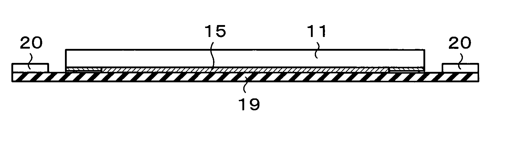
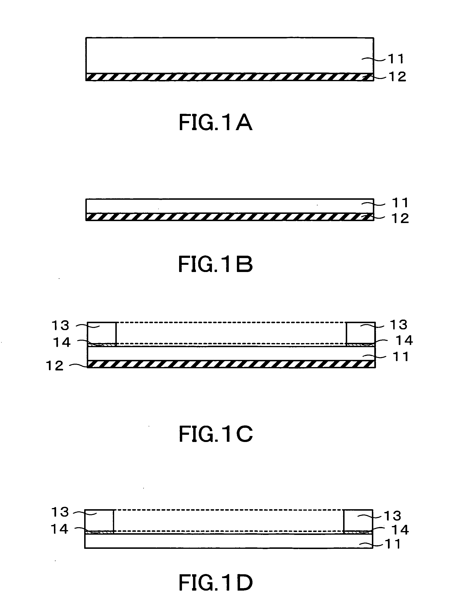
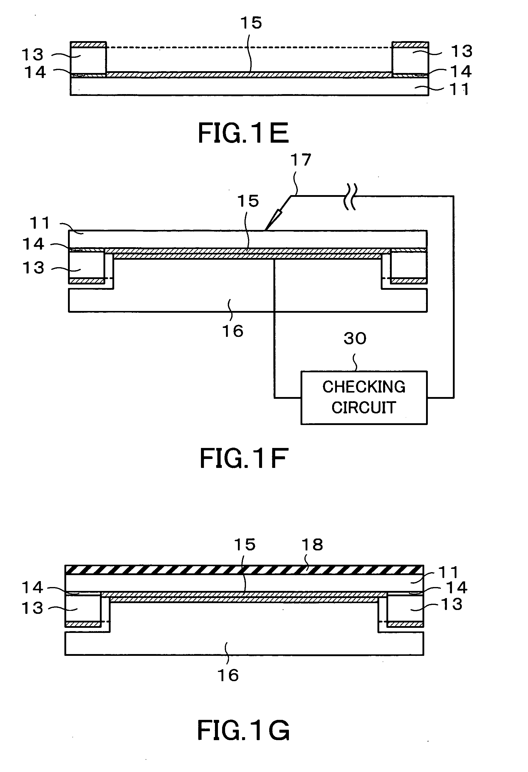
[0041] An explanation is given of a semiconductor device manufacturing method and a ring-shaped reinforcing member used therein according to this embodiment with reference to FIGS. 1A to 1G and FIG. 2.

[0042] First of all, a semiconductor substrate (semiconductor wafer) 11 is prepared as illustrated in FIG. 1A. The semiconductor substrate 11 is formed of for example, a single crystal silicon, and has a substantially circular shape with a size of, for example, a thickness of 500 μm and a diameter of 15 mm (6 inches). In a surface region of one surface of the semiconductor substrate 11, multiple semiconductor regions (not shown) for forming multiple semiconductor devices are formed by impurity diffusion and the like. Moreover, on one surface of the semiconductor substrate 11, a metallic film (not shown) is formed by sputtering, vacuum deposition, etc. The metallic film forms one end of the electrode of the semiconductor device, for example, an emitter electrode and a ...

Example

Second Embodiment

[0076] This embodiment explains a semiconductor device manufacturing method when the reinforcing ring 13 is adhered to the semiconductor substrate 11 with heat resistance resin, which is formed of polyimide, in place of the inorganic adhering material layer 14. The semiconductor device manufacturing method of this embodiment will be explained below with reference to FIGS. 3A to 3G.

[0077] First of all, the semiconductor substrate 11 is prepared. Similar to the first embodiment, multiple semiconductor devices are formed on the semiconductor substrate 11. Moreover, electrodes are formed on one surface of the semiconductor substrate 11.

[0078] Next, the first tape member 12 is adhered to one surface of the semiconductor substrate 11 with, for example, an ultraviolet curable adhesive and the semiconductor substrate 11 is thinned. Even in this embodiment, the semiconductor substrate 11 with an original thickness of 500 μm is thinned up to 100 μm.

[0079] Sequentially, th...


PUM


Abstract

A ring-shaped reinforcing ring (13) formed of, for example, silicon, is adhered to one surface of a thinly processed semiconductor substrate (11). The reinforcing ring (13) is adhered thereto with an organic adhering material layer (14) formed of a metal or alloy with a relatively low melting point or polyimide resin with a relatively low melting point or softening point. Forming a metallic film (15) is executed in a state that the reinforcing ring (13) is adhered to the semiconductor substrate (11). The reinforcing ring (13) has the same outer diameter as that of the semiconductor substrate (11). Moreover, since a total thickness of the thinly processed semiconductor substrate (11) and the reinforcing ring (13) is substantially equal to that of the semiconductor substrate (11) which is not thinly processed, the semiconductor substrate (11) to which the reinforcing ring (13) is adhered can be transferred by the existing transferring unit.

Description

TECHNICAL FIELD [0001] The present invention relates to a method for manufacturing a semiconductor device having a relatively thin semiconductor substrate and ring-shaped reinforcing member used therein. BACKGROUND ART [0002] For example, a power semiconductor device such as a power transistor or the like includes a semiconductor substrate having multiple semiconductor regions formed thereon and electrodes formed on both surfaces of the semiconductor substrate. [0003] Some of power semiconductor devices are miniaturized and thinned in accordance with miniaturization of electronic equipment. The power semiconductor devices of this type generally include a relatively thin semiconductor substrate. [0004] Conventionally, the power semiconductor device having a thin semiconductor substrate is manufactured by, for example, the following processes. [0005] First of all, as illustrated in FIG. 4A, a semiconductor substrate 100 is prepared. In a surface region of one surface of the semiconduc...

Claims


Application Information

Patent Timeline
IPC IPC(8): H01L21/02H01L21/301H01L21/304H01L21/68H01L21/78
CPCH01L21/6835H01L21/6836H01L2221/6834H01L2221/68327H01L21/78
Inventor MITA, HUMIAKI
Owner SANKEN ELECTRIC CO LTD
Why Eureka
Try Eureka