Multi-layer interconnection circuit module and manufacturing method thereof

a multi-layer interconnection and circuit module technology, applied in the direction of printed circuit board laminated, printed element electric connection formation, non-metallic protective coating application, etc., can solve the problems of difficult realization of miniaturization, shortened wiring pattern, and difficult application of multi-layer manufacturing process to typical multi-layer wiring board manufacturing process, etc., to achieve shorten the length of the wiring, reduce the attenuation of signals caused to undergo transmission, and high resolution

Inactive Publication Date: 2005-11-10
SONY CORP
View PDF6 Cites 17 Cited by
  • Summary
  • Abstract
  • Description
  • Claims
  • Application Information

AI Technical Summary

Benefits of technology

[0011] An object of the present invention is to provide a novel multi-layer interconnection (wiring) circuit module and a manufacturing method thereof which can solve problems that conventional multi-chip circuit modules as described above have.
[0012] Another object of the present invention is to provide a multi-layer interconnection (wiring) circuit module and a manufacturing method thereof in which respective unit wiring layers have fine and high density wiring patterns and have Via-on-Via structure so that interlayer connection is conducted by the shortest wiring length, miniaturization and thin structure can be realized, and high speed processing and improvement in reliability can be realized.
[0014] In accordance with the multi-layer interlayer circuit module according to the present invention, photo-lithographic processing by simple equipment and work are respectively implemented to the first and second insulating layers formed as film by photosensitive insulating resin material to form via hole grooves and wiring grooves which have high resolution. From this fact, it becomes possible to form micro via holes and / or fine and high density wiring pattern. In accordance with the multi-layer interconnection (wiring) circuit module, respective unit wiring layers are interlayer-connected to each other at the shortest distance by Via-on-Via structure so that they are laminated and formed to thereby shorten wiring length. As a result, attenuation of signals caused to undergo transmission is reduced, and signal delay is minimized. In addition, thin structure is realized, thus making it possible to cope with, e.g., large capacity, high speed and high density bus.
[0016] In accordance with the manufacturing method for multilayer interconnection circuit module according to the present invention, photo-lithographic processing is implemented to the first and second insulating layers formed as film by photosensitive insulating resin material to form via hole grooves and wiring grooves which have high resolution. From this fact, it becomes possible to form micro via holes and / or fine and high density wiring patterns. By using this manufacturing method, respective unit wiring layers are interlayer-connected to each other at the shortest distance by Via-on-Via structure so that they are laminated and formed to thereby shorten wiring length. As a result, attenuation of signals caused to undergo transmission is reduced, signal delay is minimized, and thin structure can be realized. Thus, it is possible to manufacture multi-layer interconnection (wiring) circuit module in which, e.g., measure for large capacity, high speed and high density bus has been realized.

Problems solved by technology

In this wiring formation method, it is necessary to implement precise first dry etching processing and precise second dry etching processing having depths of groove different from each other, and it is difficult to apply this method to manufacturing process for typical multi-layer wiring board.
In addition, in accordance with this wiring formation method, since wiring layers are formed on silicon substrate as multi-layer structure, there are the problem that the mounting structure onto mother board, etc. becomes complicated so that realization of miniaturization becomes difficult, and wiring pattern is also elongated.

Method used


Image

  • Multi-layer interconnection circuit module and manufacturing method thereof
  • Multi-layer interconnection circuit module and manufacturing method thereof
  • Multi-layer interconnection circuit module and manufacturing method thereof

Examples


Embodiment Construction

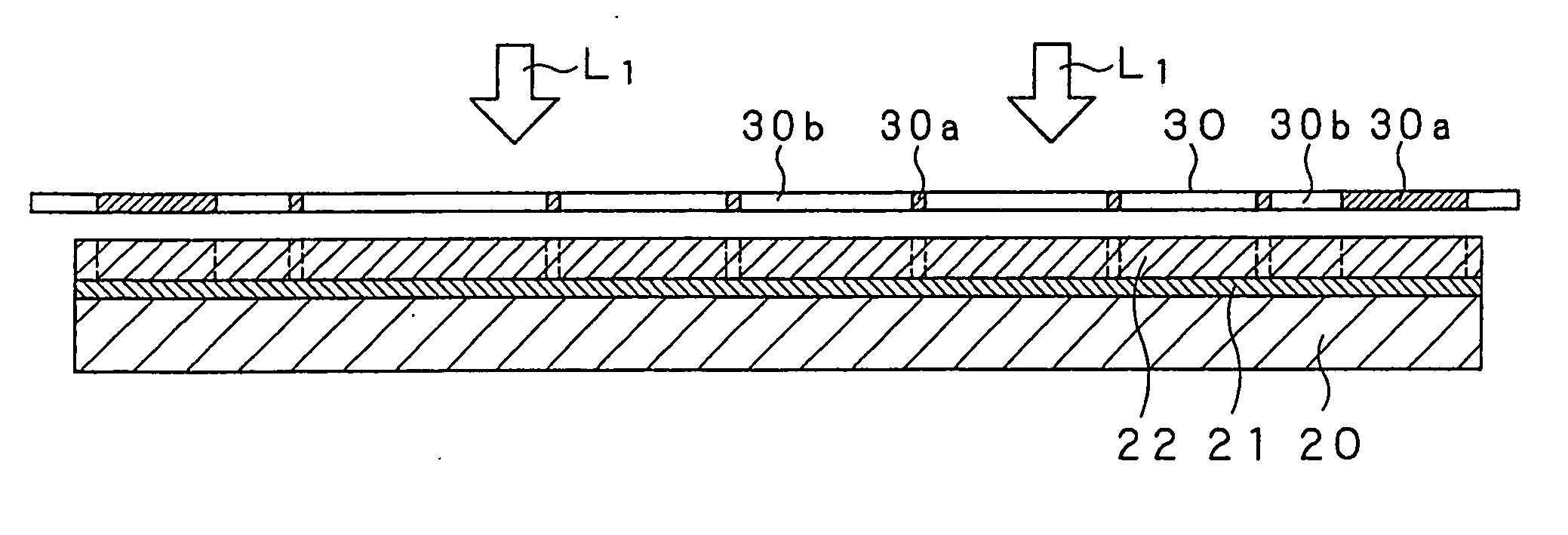
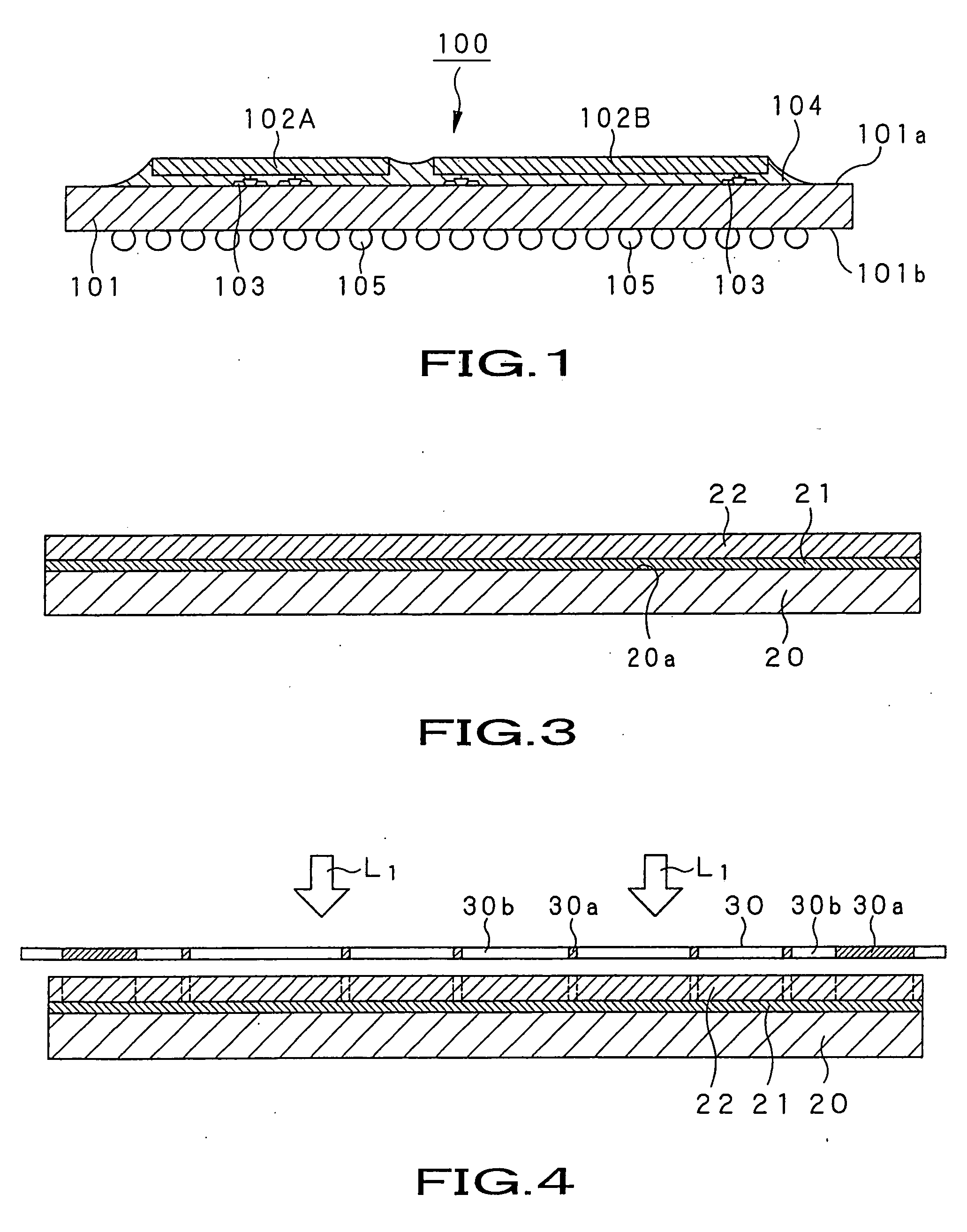
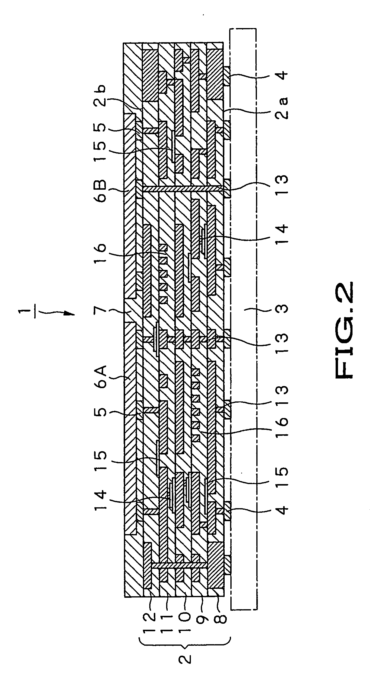
[0031] A multi-layer interconnection (wiring) circuit module (hereinafter simply abbreviated as circuit module) and a manufacturing method thereof to which the present invention is applied will now be explained with reference to the attached drawings.

[0032] The circuit module according to the present invention has, e.g., information communication function and / or storage function, etc., and is mounted in various electronic equipments such as personal computer, mobile telephone and / or audio equipment, etc., or constitutes a high frequency circuit unit of micro communication function module body attached or detached as option. At the circuit module, although its detail is omitted, there is formed a high frequency transmitting / receiving circuit unit based on the superheterodyne system for once performing conversion into intermediate frequency from transmit / receive signal, or a high frequency transmitting / receiving circuit unit based on the direct conversion system for performing transm...


PUM


Abstract

The present invention is directed to a multi-layer interconnection circuit module in which plural unit wiring layers are interlayer-connected to each other through a large number of via holes so that they are laminated and formed, wherein respective unit wiring layers (8) to (12) are adapted so that photo-lithographic processing is implemented to a first insulating layer (22) formed by photosensitive insulating resin material to form via hole grooves (25), and photo-lithographic processing is implemented to a second insulating layer (23) formed by photosensitive insulating resin material on the first insulating layer (22) to form wiring grooves (27). A conductive metal layer (24) is formed on the second insulating layer (23) in such a manner that conductive metal is filled within the via hole grooves (25) and the wiring grooves (27) to implement polishing processing to the conductive metal layer (24) until the principal surface of the second insulating layer (23) is exposed to form via holes (13) and wiring patterns (26) by the conductive metal filled within the via hole grooves (25) and the wiring grooves (27).

Description

TECHNICAL FIELD [0001] The present invention relates to a multilayer interconnection circuit module in which thin structure and high density wiring have been realized, and a manufacturing method thereof. [0002] This Application claims priority of Japanese Patent Application No. 2002-195018, field on Jul. 3, 2002, the entirety of which is incorporated by reference herein. BACKGROUND ART [0003] In various digital electronic equipments, e.g., personal computer, mobile telephone, video equipment and / or audio equipment, etc., there is provided multi-chip circuit module on which semiconductor chips such as various IC elements or LSI elements, etc. are mounted. In various digital electronic equipments, finning of circuit pattern, miniaturization of IC package, rapid improvement in integration scale, multi-pin structure and / or improvement in mounting method, etc. have been provided so that miniaturization and high level function of the multi-chip circuit module are realized. Thus, miniaturi...

Claims


Application Information

Patent Timeline
Patent Type & Authority Applications(United States)
IPC IPC(8): H01L23/12H01L21/48H01L23/538H01L25/04H01L25/18H05K3/00H05K3/20H05K3/28H05K3/42H05K3/46
CPCH01L21/4857H05K2203/0733H01L23/49822H01L23/5389H01L25/0655H01L2221/68345H01L2224/16H01L2224/73204H01L2924/01078H01L2924/01079H01L2924/15311H01L2924/18161H01L2924/19041H01L2924/3011H01L2924/3025H05K3/0023H05K3/0058H05K3/205H05K3/284H05K3/423H05K3/465H05K3/4682H05K2203/025H01L23/3121H01L23/12H01L23/48H01L23/52
Inventor OGAWA, TSUYOSHI
Owner SONY CORP
Why Eureka
Try Eureka