Laser annealing device and method for producing thin-film transistor

Inactive Publication Date: 2005-11-17
SONY CORP
View PDF25 Cites 22 Cited by
  • Summary
  • Abstract
  • Description
  • Claims
  • Application Information

AI Technical Summary

Benefits of technology

[0027] It is therefore an object of the present invention to provide an apparatus and a method for laser annealing whereby it is

Problems solved by technology

However, with the above-described heating method, a heating mechanism must be-provided, thus complicating the structure of the laser annealing device.
Moreover, the operation of heating the insulating substrate is time-consuming, thus lowering the throughput of the device.
Additionally, the substrate position is moved due to thermal expansion of the insulating substrate, attendant on the heating, so that it becomes impossible to illuminate the laser light at a correct position.
Thus, with a conventional laser annealing device, it has not been possible to increase the crystal grain size or to homogenize the crystal grain size distribution by a simplified structure.
The result is that the time period during which the crystal growth takes place is shortened, with the result that the crystal grain size cannot be increased.
However, if the designing is made such as to maximize the laser light output power, it is extremely difficult to change the pulse width, given the characteristics of the laser light source.
However, the excimer laser, used up to now for a laser annealing device, is unstable in its output, such that the pulse oscillation timing undergoes an error of not less than 100 nsec.
Thus, with the laser annealing device, employing the conventional excimer laser annealing device, it has not been possible to reduce the pulse width of the laser light source, to increase the crystal grain size of the polysilicon film and to homogenize the crystal grain size.
However, with the conventional laser annealing device, it is not possible to control the sites of generation of the crystal nuclei.
Thus, with the c

Method used


Image

  • Laser annealing device and method for producing thin-film transistor
  • Laser annealing device and method for producing thin-film transistor
  • Laser annealing device and method for producing thin-film transistor

Examples


first embodiment

[0062] As a first embodiment of the present invention, a laser annealing device performing the laser annealing, as the temperature of the insulating substrate has been raised, is now explained.

[0063] Meanwhile, the laser annealing device of the first embodiment is used in e.g., a polycrystallizing step in the manufacturing process for a thin film transistor (TFT) of forming a polysilicon film which is to become a channel layer. That is, the laser annealing device of the first embodiment is used in a step of illuminating the laser light on an amorphous silicon film formed on the glass substrate to effect annealing.

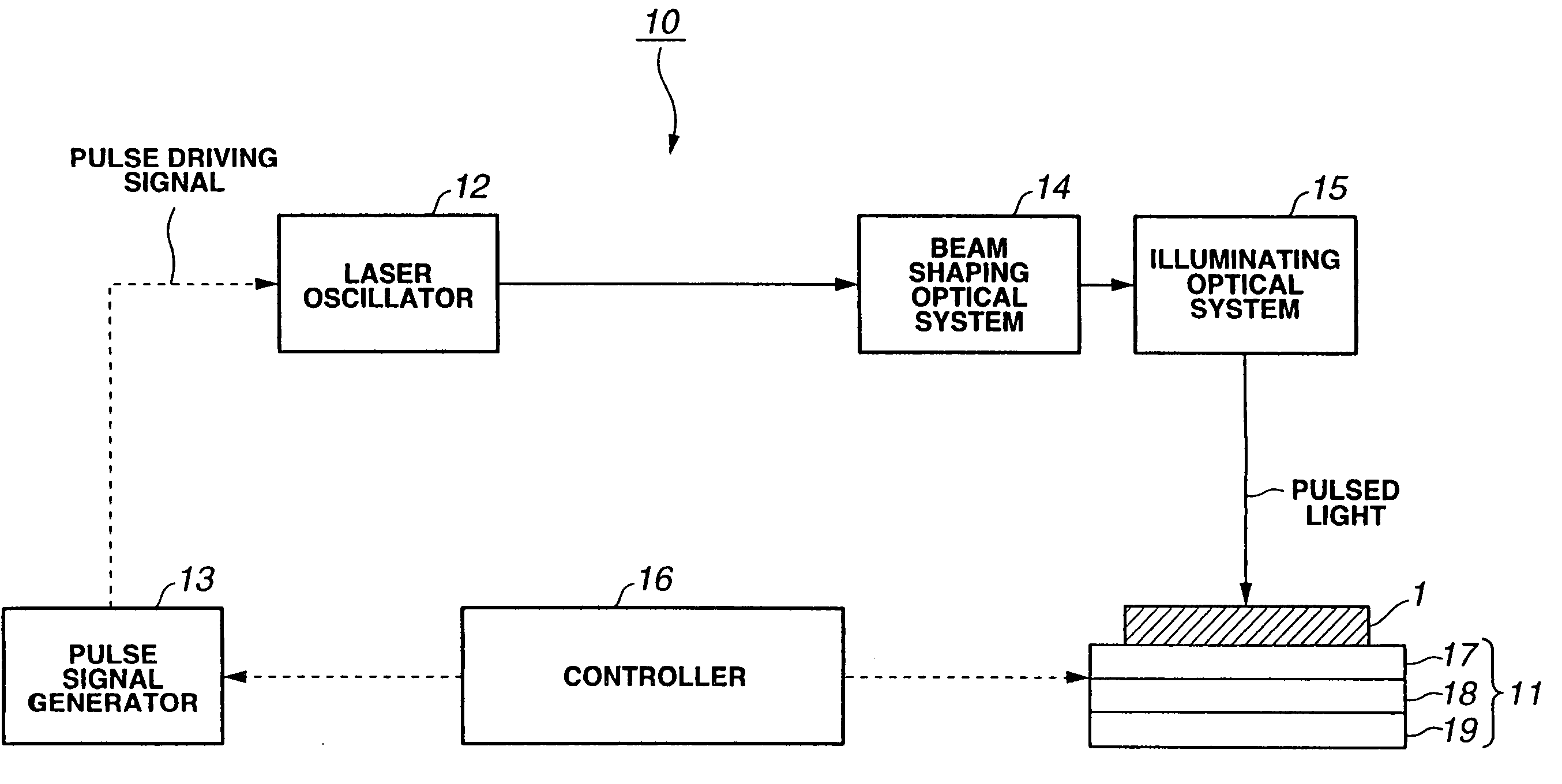
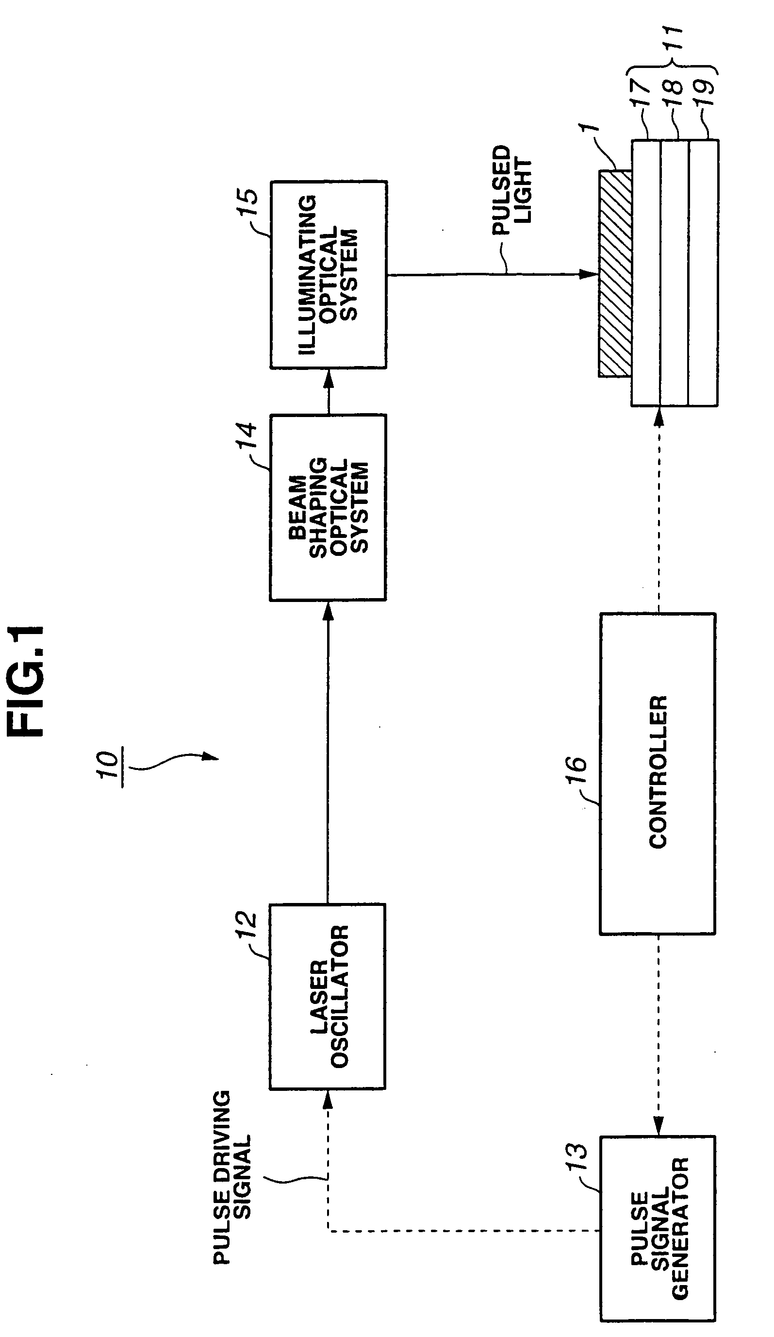
[0064]FIG. 1 shows the structure of a laser annealing device 10 of the first embodiment of the present invention. The laser annealing device 10 includes a movable stage 11, on which to set a TFT substrate 1 to be annealed, a laser oscillator 12 for radiating pulsed laser light, a pulse signal generator 13 for generating pulse driving signals of a predetermined period, a b...

second embodiment

[0104] As a second embodiment of the present invention, a laser annealing device in which plural light pulses are synthesized to generate a synthesized pulsed laser light with an elongated pulse width and in which the resulting synthesized light is illuminated on a substance, is now explained.

[0105] Meanwhile, the present second embodiment of the laser annealing device is used in a polycrystallization step of forming a polysilicon film as a channel layer in the manufacturing process for a thin film transistor (TFT). That is, the present second embodiment of the laser annealing device is used in a step of illuminating the laser light on the amorphous silicon film formed on a glass substrate to effect annealing.

[0106] In the following explanation of the second embodiment of the laser annealing device, the component parts which are the same as those of the first embodiment of the laser annealing device are depicted by the same reference numerals and the detailed description therefor ...

third embodiment

[0137] As a third embodiment of the present invention, such a laser annealing device in which it is possible to control the position of generation of crystal nuclei of a polysilicon film is hereinafter explained.

[0138] It should be noted that the laser annealing device of the third embodiment is used in a polycrystallization process for forming the polysilicon film, as a channel layer, in the manufacturing process for a thin film transistor (TFT). That is, the laser annealing device of the third embodiment is used in a step of illuminating the laser light on the amorphous silicon film formed on the glass substrate.

[0139] In the following explanation of the laser annealing device of the third embodiment, the same reference numerals as those used in the explanation of the laser annealing device 10 of the first embodiment are used, and the detailed description thereof is omitted for simplicity.

[0140]FIG. 16 shows the structure of a laser annealing device 30 according to the third em...


PUM

PropertyMeasurementUnit
Fractionaaaaaaaaaa
Fractionaaaaaaaaaa
Nanoscale particle sizeaaaaaaaaaa

Abstract

A laser annealing device (10) includes a laser oscillator (12), radiating a pulsed laser light beam of a preset period, and an illuminating optical system (15) for illuminating a pulsed laser light beam to an amorphous silicon film (1). The illuminating optical system (15) manages control for moving a laser spot so that a plural number of light pulses will be illuminated on the same location on the amorphous silicon film (1). The laser oscillator (12) radiates a laser light beam of a pulse generation period shorter than the reference period. The reference period is a time interval as from the radiation timing of illumination of a pulsed laser light beam on the surface of the film (1) until the timing of reversion of the substrate temperature raised due to the illumination of the laser light beam to the original substrate temperature.

Description

TECHNICAL FIELD [0001] This invention relates to a method and an apparatus for laser annealing by illuminating the laser light on a substance, and to a method and an apparatus for the preparation of a thin-film transistor including a laser annealing process for effecting the laser annealing. [0002] This application claims priority of Japanese Patent Application No. 2001-346454, filed on Nov. 12, 2001, Japanese Patent Application No. 2001-352162, filed on Nov. 16, 2001, Japanese Patent Application No. 2001-374921, filed on Dec. 7, 2001, and Japanese Patent Application No. 2001-373189, filed on Dec. 6, 2001, the entireties of which are incorporated by reference herein. BACKGROUND ART [0003] (1) Such a technique has been developed in which a polysilicon film is formed on an insulating substrate, such as a glass substrate or a plastics substrate to fabricate a thin-film transistor (TFT) using this polysilicon film as a channel layer. Since the single-crystal silicon substrate is expensi...

Claims


Application Information

Patent Timeline
IPC IPC(8): B23K26/06B23K26/067H01L21/20H01L21/268
CPCB23K26/0604B23K26/0613B23K26/063B23K26/067H01L21/02691H01L27/1285H01L21/02532H01L21/02678H01L21/02686H01L21/268B23K26/0622H01L29/786
Inventor IMAI, YUTAKAUMEZU, NOBUHIKOASANO, AKIHIKOHOTTA, SHINTATSUKI, KOICHIFUKUMOTO, ATSUSHIKUBOTA, SHIGEO
Owner SONY CORP
Why Eureka
Try Eureka