Laser irradiation method and method of manufacturing a semiconductor device

a semiconductor device and laser irradiation technology, applied in the direction of solid-state devices, crystal growth processes, chemistry apparatus and processes, etc., can solve the problems of high mass production, inability to control the position of large crystal grains, and hardly possible channel forming regions, so as to improve the performance of semiconductor devices, reduce the number of crystal grain boundaries that may be contained in channel forming regions, and increase the grain size of crystal grains

Inactive Publication Date: 2007-05-15
SEMICON ENERGY LAB CO LTD
View PDF23 Cites 67 Cited by
  • Summary
  • Abstract
  • Description
  • Claims
  • Application Information

AI Technical Summary

Benefits of technology

[0044]The performance of the semiconductor device can be remarkably improved by obtaining the crystalline semiconductor film having the crystal grains of large grain size. For example, regarding a TFT given as an example, the number of crystal grain boundaries that may be contained in a channel forming region can be reduced with enlarged grain size of a crystal grain. That is, the TFT having the channel forming region with one crystal grain boundary, preferably zero crystal grain boundary can be manufactured. Further, since an individual crystal grain has the crystallinity such that it can be regarded substantially as a single crystal, the high mobility (field effect mobility) equal to or more than that of a transistor using a single crystal semiconductor can be obtained.
[0045]Furthermore, since the number of crossings across the crystal grain boundary by a carrier can be remarkably reduced, it is possible to reduce variations of an on current value (a value of a drain current flowing in an on state of a TFT), an off current value (a value of a drain current flowing in an off state of a TFT), a threshold voltage, an S value and an electric field mobility.

Problems solved by technology

In particular, when the linear beam is used, laser irradiation can be conducted over the entire irradiation surface with scanning only in a direction perpendicular to the longitudinal direction of the linear beam, which is different from the case where the spot laser beam that requires scanning in the front and rear directions and in the right and left directions is used, which leads to high mass production.
However, it is hardly possible that the channel forming region is formed of a single crystal semiconductor film without influence of the crystal grain boundary.
However, the above-mentioned energy region is very narrow, and the position where a large crystal grain is obtained can not be controlled.
However, gases such as Kr (krypton) and Xe (xenon) are very costly.
Thus, there is a problem in that an increase of manufacturing cost is incurred with the high frequency of gas exchange.
Many of these attached devices are expensive, and there is also a problem in that the increase of manufacturing cost is incurred.
However, the maintenance involves a lot of trouble, and also, there is a defect that the laser irradiation apparatus has high running cost (here, the running cost indicates the cost generated with operation) as a laser irradiation apparatus for mass production.
Therefore, the life of the LD becomes short, and as a result, the LD excitation costs highly in comparison with the flash lamp excitation.
However, in the oscillation by the flash lamp excitation, electrons excited by instantaneously input energy are released all at once, and thus, the laser output time becomes very short.
Therefore, it is difficult that the formation of the crystal grain, of which the grain size is equal to or larger than that of the crystal grain formed by laser crystallization using the excimer laser, is realized by laser crystallization using the solid laser.
Further, there is a problem on throughput in the case where the SLS method is used in manufacturing a TFT applied to a liquid crystal display having a large surface area.

Method used


Image

  • Laser irradiation method and method of manufacturing a semiconductor device
  • Laser irradiation method and method of manufacturing a semiconductor device
  • Laser irradiation method and method of manufacturing a semiconductor device

Examples


embodiment mode 1

[0075]An embodiment mode of the present invention is described below with reference to FIGS. 7A to 8B.

[0076]First, an example of a method of manufacturing a reflecting member is described with reference to FIG. 7A. In FIG. 7A, as a substrate 20, a glass substrate or a synthetic quartz glass substrate is used. Further, a plastic substrate having heat resistance that withstands a process temperature may be used.

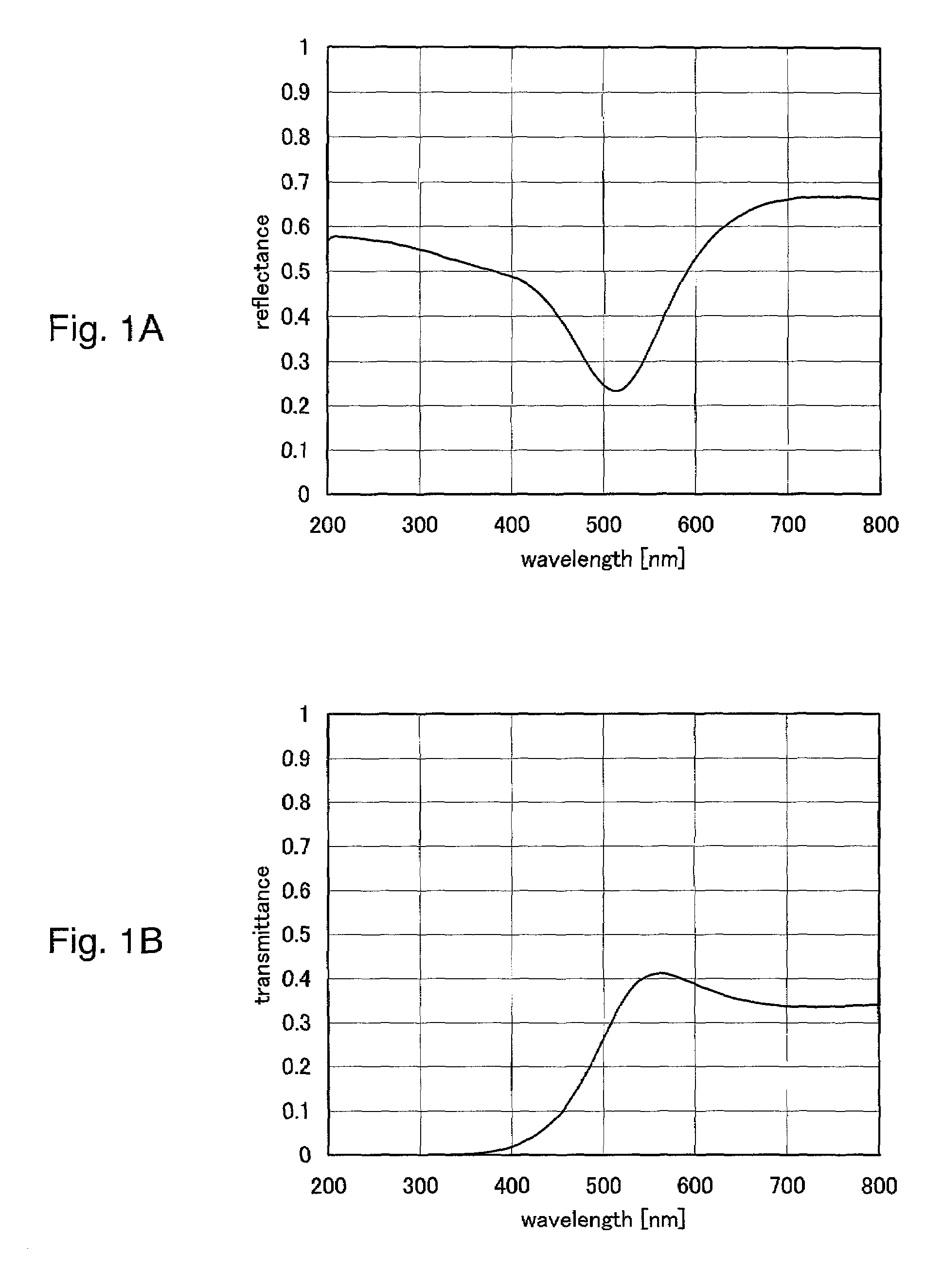
[0077]Then, a reflecting film 21 is deposited on the substrate 20 by a known means (a sputtering method, an LPCVD method, a plasma CVD method or the like). As the reflecting film 21, a film with high reflectivity to a wavelength of a laser beam used in crystallization and also with heat resistance that withstands the process temperature is desirable. The reflectivity most suitable for crystallization depends on the state of a semiconductor film, the wavelength of the laser beam and the like.

[0078]As described above, the reflecting member is manufactured. Of course, instead of m...

embodiment mode 2

[0084]Another structure of the present invention, which is different from that of Embodiment Mode 1, is described below with reference to FIGS. 22A to 24E.

[0085]First, a method of manufacturing a reflecting member is described with reference to FIGS. 22A and 22B. In FIGS. 22A and 22B, as a substrate 220, a glass substrate or a synthetic quartz glass substrate is used. Further, a plastic substrate having heat resistance that withstands a process temperature may be used.

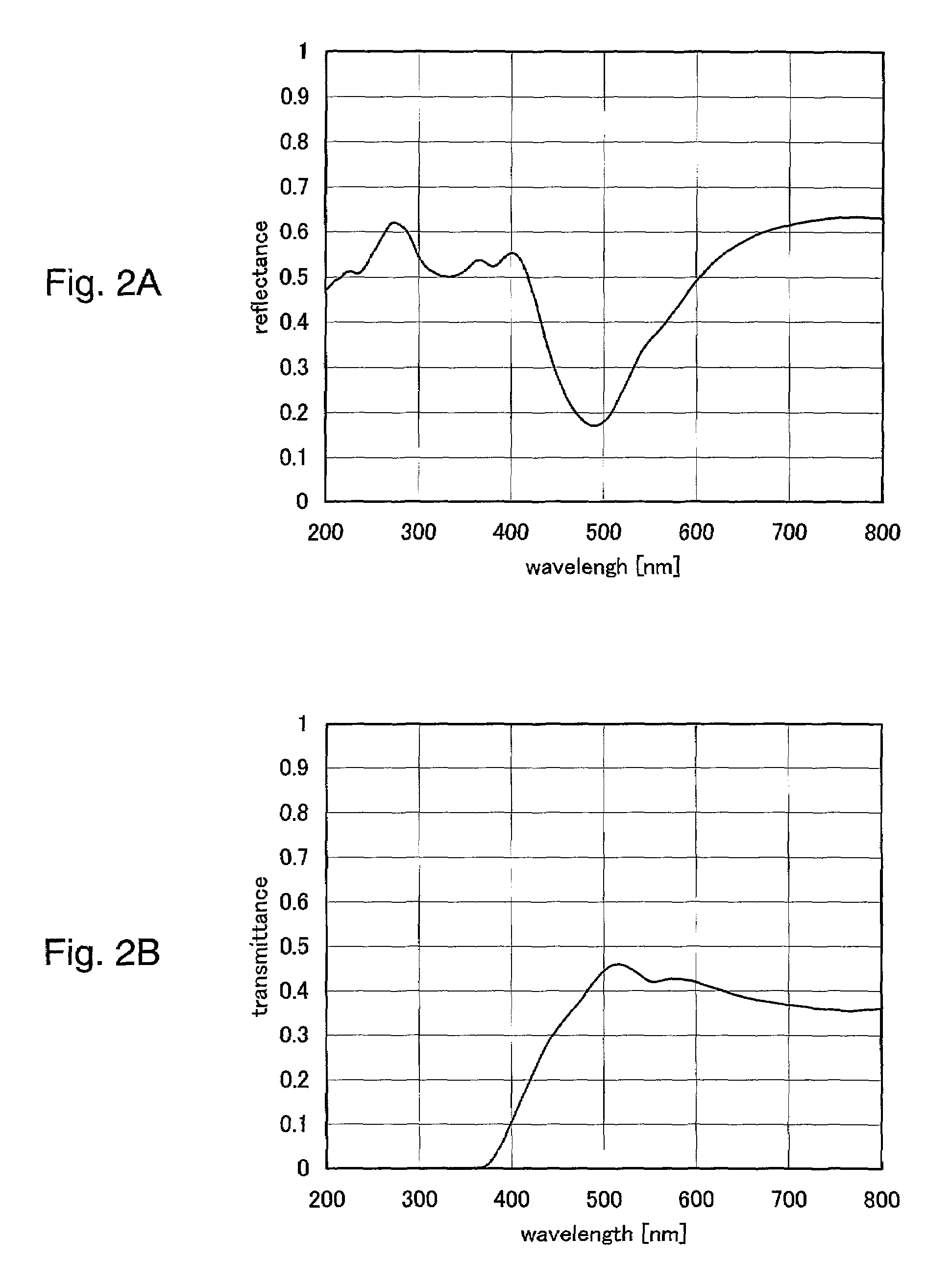
[0086]Then, a reflecting film 221 is deposited on the substrate 220 by a known means (a sputtering method, an LPCVD method, a plasma CVD method or the like). As the reflecting film 221, a film with high reflectivity to a wavelength of a laser beam used in crystallization and also with heat resistance that withstands the process temperature is desirable. The reflectivity most suitable for crystallization depends on the state of a semiconductor film, the wavelength of the laser beam and the like.

[0087]Thereafter, the ref...

embodiment 1

[0098]An embodiment of the present invention is described below with reference to FIGS. 7A to 8B.

[0099]First, a method of manufacturing a reflecting member is described with reference to FIG. 7A. In FIG. 7A, as a substrate 20, a glass substrate or a synthetic quartz glass substrate is used. Further, a plastic substrate having heat resistance that withstands a process temperature may be used. In this embodiment, 1737 substrate glass of Corning Corp. is used.

[0100]Then, a reflecting film 21 is deposited on the substrate 20 by a known means (a sputtering method, an LPCVD method, a plasma CVD method or the like). As the reflecting film 21, a film with high reflectivity to a wavelength of a laser beam used in crystallization and also with heat resistance that withstands the process temperature is desirable. The reflectivity most suitable for crystallization depends on the state of a semiconductor film, the wavelength of the laser beam and the like. In this embodiment, tantalum (Ta) is fo...


PUM

PropertyMeasurementUnit
wavelengthsaaaaaaaaaa
lengthaaaaaaaaaa
distanceaaaaaaaaaa

Abstract

A crystalline semiconductor film having crystal grains of large grain size or crystal grains in which the position and the size are controlled is formed to manufacture a TFT, whereby a semiconductor device that enables a high-speed operation is realized. First, a reflecting member is provided on a rear surface side of a substrate on which a semiconductor film is formed (semiconductor film substrate). When a front surface side of the semiconductor film substrate is irradiated with a laser beam that penetrates the semiconductor film substrate, the laser beam is reflected by the reflecting member to irradiate the semiconductor film from the rear surface side. With this method, an effective energy density is raised in the semiconductor film, and an output time is made long. Thus, the cooling rate of the semiconductor film is made gentle and crystal grains of large grain size are formed. Further, the front surface side of the semiconductor film substrate is irradiated with the laser beam by using a substrate on which a reflecting layer is partially formed as the reflecting member, whereby the semiconductor film is partially irradiated with the laser beam from the rear surface side. Thus, a temperature distribution is generated in the semiconductor film, and the location where a lateral growth is generated and the lateral direction can be controlled. Therefore, the crystal grains of large grain size can be obtained.

Description

BACKGROUND OF THE INVENTION[0001]1. Field of the Invention[0002]The present invention relates to a laser irradiation method of annealing a semiconductor film using a laser beam (hereinafter referred to as laser annealing) and a laser irradiation apparatus for performing the laser annealing (apparatus including a laser and an optical system for guiding a laser beam output from the laser to a member to be processed). Further, the present invention relates to a semiconductor device manufactured by the steps including the laser annealing step and a method of manufacturing the semiconductor device. Note that the semiconductor device mentioned through the specification includes an electro-optical device such as a liquid crystal display device or a light emitting device and an electronic device including the electro-optical device as its component.[0003]2. Description of the Related Art[0004]In recent years, techniques of crystallizing a semiconductor film formed on an insulating substrate...

Claims


Application Information

Patent Timeline
Patent Type & Authority Patents(United States)
IPC IPC(8): H01L21/00C30B1/00H01L21/20H01L21/268H01L21/77
CPCH01L21/2026H01L21/268H01L27/1285H01L27/1281H01L21/02592H01L21/02686H01L21/02683H01L21/02502H01L21/02678H01L21/02488H01L21/02422H01L21/02532H01L21/02595H01L21/02691
Inventor KAWASAKI, RITSUKONAKAJIMA, SETSUO
Owner SEMICON ENERGY LAB CO LTD
Why Eureka
Try Eureka