Semiconductor micro device

a semiconductor and micro-chip technology, applied in the direction of turning-sensitive devices, acceleration measurement using interia forces, liquid/fluent solid measurement, etc., can solve the state and distribution of thermal strain potentially imposed on the silicon structure chip, the structure chip erroneously operates, and the thermal strain of the structure chip is more complex. , to achieve the effect of reducing the area of contact, increasing the thermal strain of the structure chip, and reducing the thermal strain potentially imposed on the structure chip

Inactive Publication Date: 2005-11-17
MITSUBISHI ELECTRIC CORP
View PDF13 Cites 7 Cited by
  • Summary
  • Abstract
  • Description
  • Claims
  • Application Information

AI Technical Summary

Benefits of technology

[0016] In the present invention, it was discovered that, with the contact portion of the die pad being formed along the direction of diagonal line of the rectangular structure chip, thermal strain of the structure chip tends to increase. Therefore, the die pad of the lead frame used in the present invention is designed to reduce the area of contact portion that are to be formed in a position corresponding to the diagonal line of the structure chip. Consequently, in the die pad used in the present invention, the non-contact portion is formed in a portion or the entirety of the region corresponding to the diagonal line of the structure chip.
[0017] According to the present invention, the area of the contact portion formed in a position corresponding to the diagonal line of the structure chip is reduced, whereby the thermal strain potentially imposed on the structure chip is reduced. Thereby, a high-reliability semiconductor micro device can be obtained.
[0018] The non-contact portion is filled with the resin encapsulating material by the resin encapsulation step. As a result, in the state where the semiconductor micro device is manufactured into a final product, the structure chip therein is not only supported by the contact portion, but is also supported by the resin encapsulating material. Consequently, compared with a semiconductor micro device wherein the clearance remains in the non-contact portion without encapsulation by resin material, impact resistance of the structure chip of the present invention is improved.

Problems solved by technology

The thermal expansion difference causes tensile stress or compression stress in the silicon structure chip, thereby potentially leading to distortion, that is, thermal strain of the chip.
With advances in miniaturization technology in the field of silicon structure chip s, even fine thermal strain causes a critical problem in that the silicon structure chip erroneously operates.
As such, in comparison to a conventional non-resin-encapsulated micro device, the state and distribution of thermal strain potentially imposed on the silicon structure chip are more intricate.
For this reason, in the encapsulated micro device, the thermal strain cannot be sufficiently relieved or removed by the conventional method.
As a result, the difference of the encapsulated micro device implies that thermal strain potentially imposed on the sensor chip is significantly higher.
In this case, however, since the sensor chip cannot be securely boded with die (“die-bonded”, hereafter), the chip is shaky during the manufacturing, thereby potentially leading to an increase of a defective-product occurrence rate.

Method used


Image

  • Semiconductor micro device
  • Semiconductor micro device
  • Semiconductor micro device

Examples


first embodiment

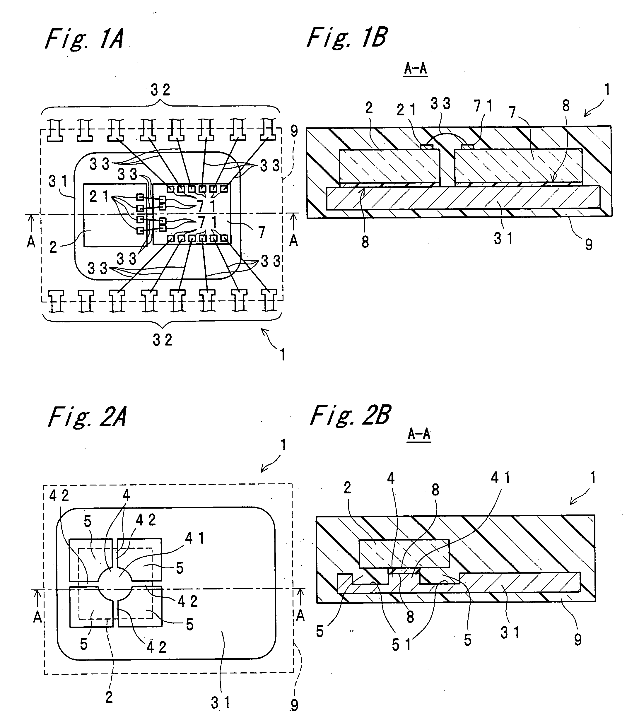
[0056]FIGS. 1A and 1B show schematic views of a resin-encapsulated semiconductor micro device 1. A sensor chip 2 as a silicon structure chip having a movable portion, and a semiconductor chip 7 (application specific integrated circuit (ASIC)) are die-bonded on a die pad 31 of a lead frame. The sensor chip 2 and the semiconductor chip 7 are electrically connected to each other by wires 33 through bonding pads 21 and 71 provided on the surfaces of the sensor chip 2 and the semiconductor chip 7 respectively. Further, the semiconductor chip 7 is electrically connected by wires 33 to inner leads 32 of the lead frame. The sensor chip 2, the semiconductor chip 7, the die pad 31, and the inner leads 32 are molded of a resin encapsulating material 9 and thereby hermetically sealed from the outside.

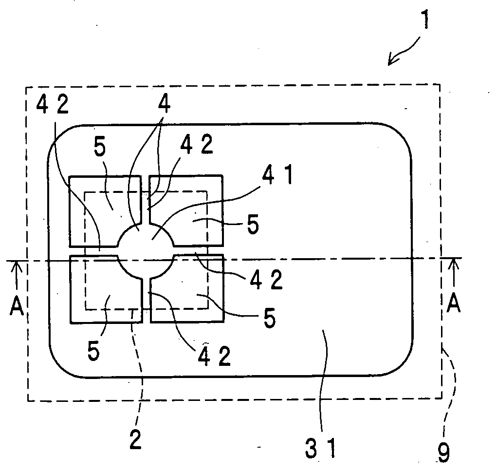
[0057]FIG. 2A is view of a first embodiment of the semiconductor micro device according to the present invention. More specifically, FIG. 2 mainly shows configurations of a sensor chip 2 and a die...

second embodiment

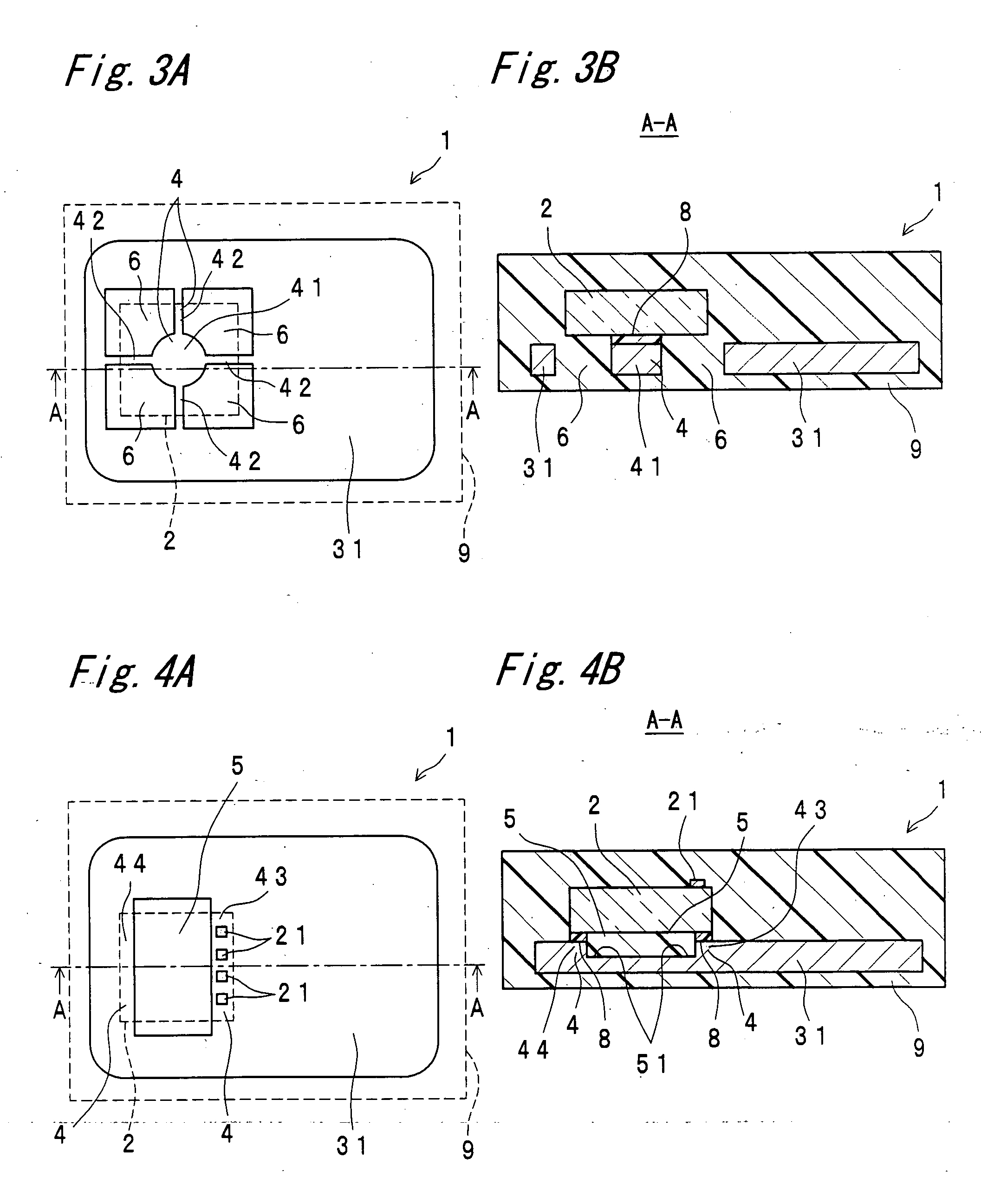
[0071]FIG. 4A is view of a second embodiment of the semiconductor micro device according to the present invention. More specifically, FIG. 4A mainly shows configurations of a sensor chip 2 and a die pad 31, wherein a semiconductor chip 7 and inner leads 32 are not shown. The sensor chip 2 used in the present embodiment is shaped to be electrically communicable with another semiconductor chip 7 by wire bonding. In the shown sensor chip 2, four bonding pads 21 for wire bonding are formed on the upper surface of the sensor chip 2 along one side of the rectangle whereon the sensor chip 2.

[0072] A contact portion 4 for supporting the sensor chip 2 and a recess portion 5 formed by etching about half the thickness of the die pad 31 are formed on the surface of the die pad 31.

[0073] The contact portion 4 is constituted of two portions. One is a pad support portion 43 that supports a bottom portion of one side (right side of the chip, as viewed in FIG. 4A), along which the bonding pads 21 ...

third embodiment

[0089]FIG. 7A is view of a third embodiment of the semiconductor micro device according to the present invention. More specifically, FIG. 7A mainly shows configurations of a sensor chip 2 and a die pad 31, wherein a semiconductor chip 7 and inner leads 32 are not shown. The sensor chip 2 used in the present embodiment is shaped to be electrically communicable with another semiconductor chip 7 by wire bonding, as in the case of FIG. 1A. In the shown sensor chip 2, four bonding pads 21 for wire bonding are formed on the upper surface of the sensor chip 2 along one side of the rectangle whereon the sensor chip 2.

[0090] A contact portion 4 for supporting the sensor chip 2 and a recess portion 5 formed by etching about half the thickness of the die pad 31 are formed on the surface of the die pad 31.

[0091] The contact portion 4 is constituted of two portions. One is a pad support portion 43 that supports a bottom portion of one side (right side of the chip, as viewed in FIG. 7A), along ...


PUM

PropertyMeasurementUnit
thermal strainaaaaaaaaaa
resistanceaaaaaaaaaa
accelerationaaaaaaaaaa

Abstract

A semiconductor micro device is provided with a rectangular silicon micro structure chip; a lead frame having a die pad for securing the silicon structure chip comprising a contact portion with the chip; and a resin encapsulating material for encapsulating the silicon structure chip and part of the lead frame; wherein the die pad of the lead frame has a non-contact portion positioned lower than the contact portion not to be in contact with the silicon structure chip, the non-contact portion being formed at least in a position corresponding to a diagonal portion of the silicon structure chip. A clearance between the non-contact portion and the silicon structure chip is filled with the resin encapsulating material, whereby the die pad and the silicon structure chip are bonded to each other by the resin encapsulating material.

Description

BACKGROUND OF THE INVENTION [0001] 1. Field of the Invention [0002] The present invention relates generally to resin-encapsulated semiconductor micro devices each having a silicon micro structure chip, and more particularly to a micro device capable of relieving thermal strain potentially imposed on a silicon structure chip. [0003] 2. Description of the Related Art [0004] Silicon micro structure chips having micro movable components are used as, for example, acceleration sensors and angular acceleration sensors for sensing accelerations of motor vehicles, aircrafts, and the like; and electrostatic actuators formed by utilizing micro-processing techniques. For example, a sensor chip for an acceleration sensor has a cantilevered movable portion and a static portion disposed in proximity to the movable portion. When operation enters an acceleration state, the movable portion of the sensor chip finely moves to sense a fine distance transition between the movable portion and the static p...

Claims


Application Information

Patent Timeline
Patent Type & Authority Applications(United States)
IPC IPC(8): H01L23/28B81B1/00B81C3/00G01C19/56G01C19/58G01P15/08H01L23/00H01L23/495H01L23/50
CPCH01L23/49503H01L2224/32245H01L24/32H01L2224/32014H01L2224/48091H01L2224/48137H01L2224/48247H01L2224/49171H01L2224/49175H01L2224/73265H01L2924/01005H01L2924/01013H01L2924/01029H01L2924/01033H01L2924/01082H01L2924/14H01L2924/1433H01L2924/19043H01L2924/30105H01L2924/01068H01L2924/01006H01L24/48H01L24/49H01L23/49513H01L2924/00014H01L2924/00H01L2924/181H01L2224/05553H01L2224/83385H01L2224/05554H01L2224/32055H01L2924/00012H01L2224/45099H01L2224/45015H01L2924/207A47J37/067A47J36/02
Inventor OTANI, HIROSHI
Owner MITSUBISHI ELECTRIC CORP
Why Eureka
Try Eureka