

Method for manufacturing resonator
a manufacturing method and resonator technology, applied in the field of resonators, can solve the problems of reducing the step yield, deteriorating the performance of the fbars, and affecting the performance of the fbars, and achieves the effects of reducing the cost of resonators, and uniform crystallinity
- Summary
- Abstract
- Description
- Claims
- Application Information
AI Technical Summary
Benefits of technology
Problems solved by technology
Method used
Image

Examples
embodiment 1
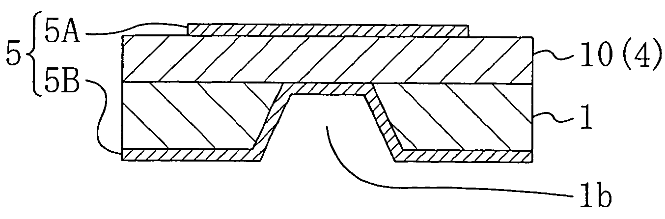
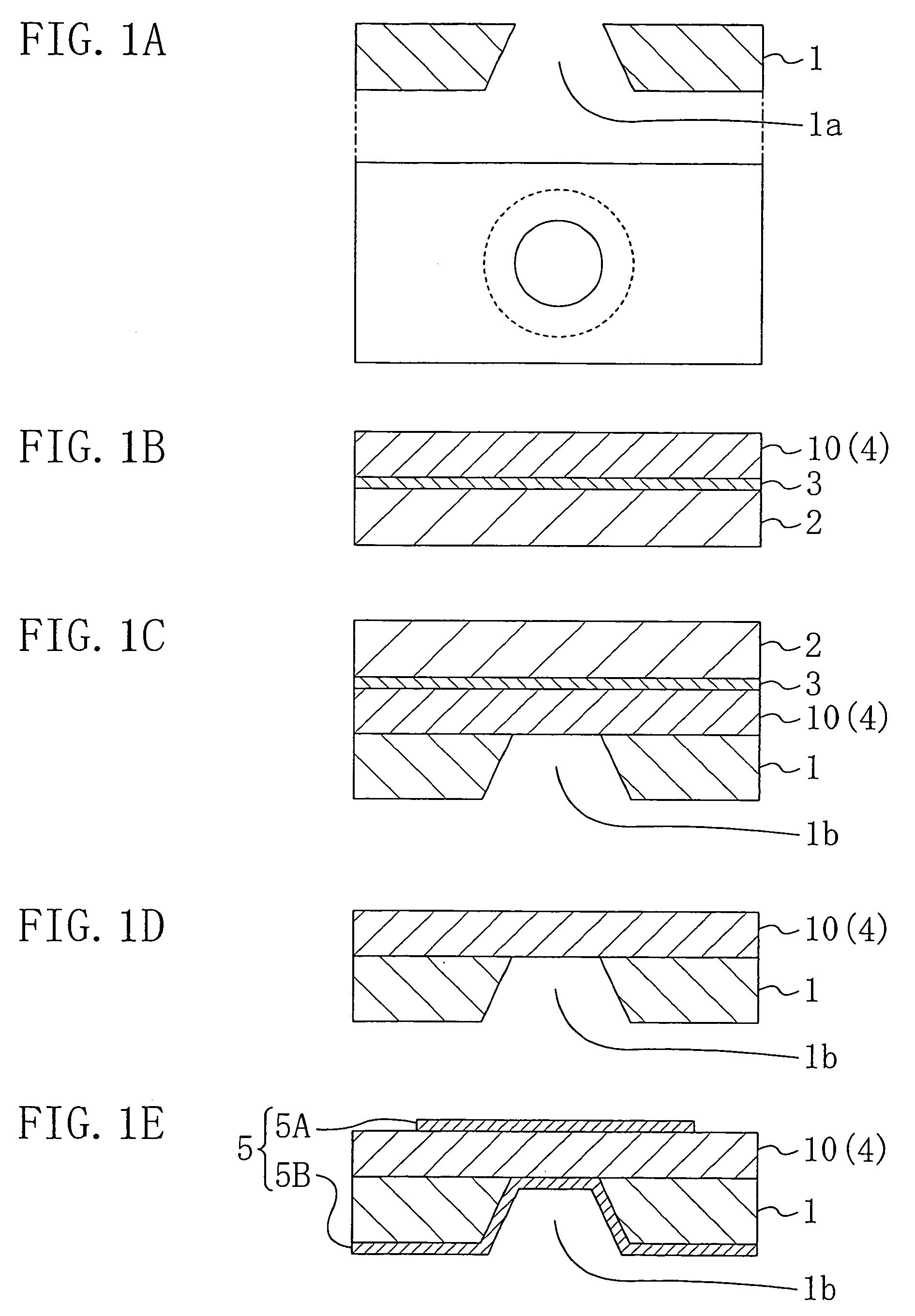
[0058] Referring to FIG. 1A to 1E, an explanation is given for Embodiment 1 of the present invention. FIGS. 1A to IE schematically illustrate the steps of manufacturing a film bulk acoustic resonator (FBAR) of this embodiment.
[0059] First, as shown in FIG. 1A, a resonator substrate 1 made of silicon (Si) is irradiated with the third harmonic of a yttrium aluminum garnet (YAG) laser (wavelength: 355 nm, output: 300 J / cm2) to form a through hole 1a penetrating the resonator substrate 1.
[0060] Then, as shown in FIG. 1B, a buffer layer 3 made of gallium nitride (GaN) is formed on a preparation substrate 2 made of silicon carbide (SiC). Then, a piezoelectric film 4 made of aluminum nitride (AlN) is deposited thereon by epitaxial growth. In this embodiment, the piezoelectric film 4 solely serves as a resonator film 10.
[0061] The resonator film 10 is brought into close contact with the main surface of the resonator substrate 1 and then heated at 375° C. for 10 minutes so that the resona...
first alternative example of embodiment 1
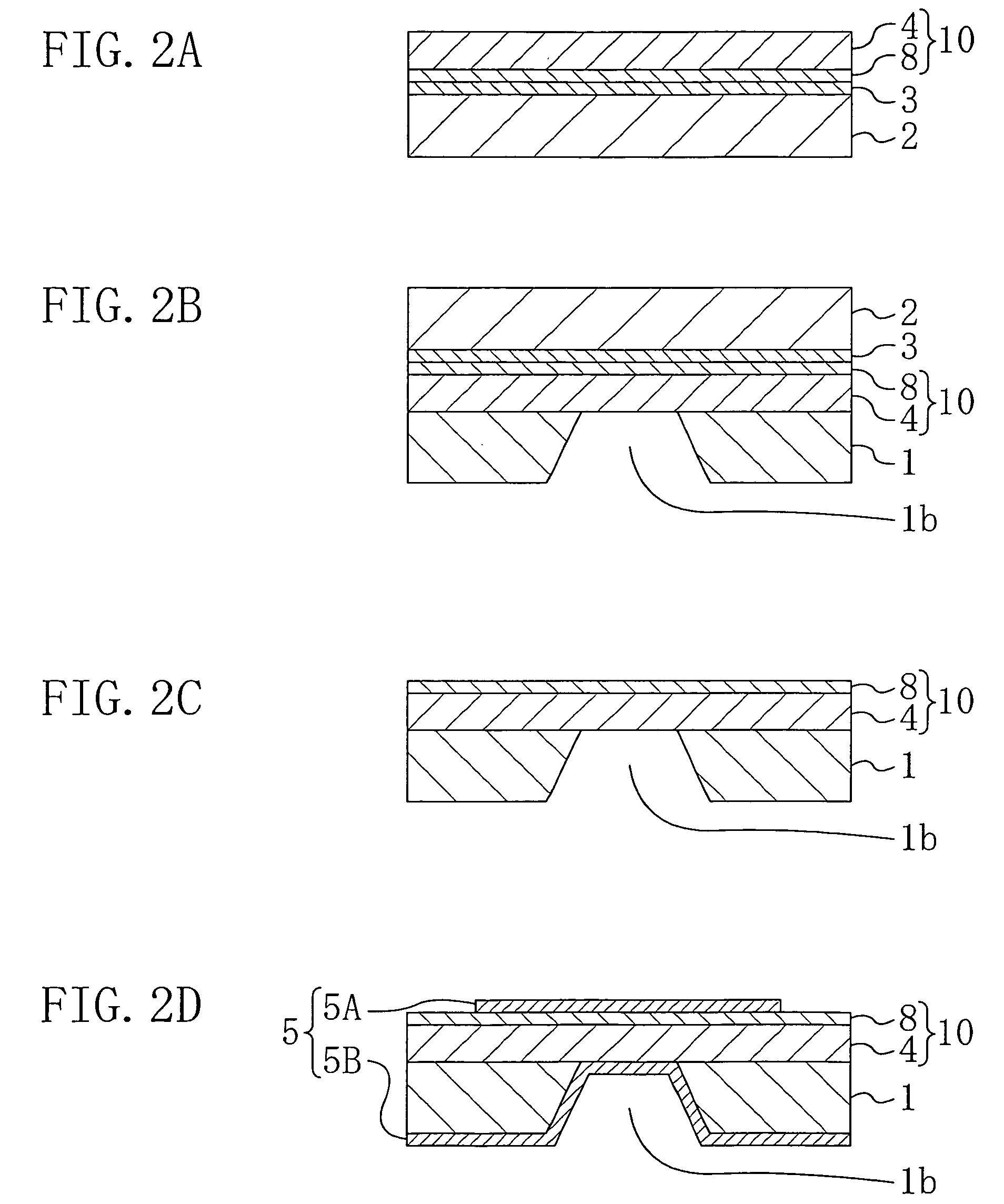
[0075] Hereinafter, with reference to FIGS. 2A to 2D, an explanation is given for a first alternative example of Embodiment 1. FIGS. 2A to 2D schematically illustrate the method for manufacturing the resonator of this alternative example. In FIGS. 2A to 2D, the same components as those shown in FIGS. 1A to 1E are given with the same reference numerals. In this alternative example, the steps prior to the step of forming the through hole 1a in the resonator substrate 1 are the same as those in Embodiment 1 and therefore the explanation thereof is omitted.
[0076] First, as shown in FIG. 2A, a buffer layer 3 made of GaN is formed on a preparation substrate 2 made of SiC. Then, an insulating film made of silicon oxide (SiO2) as a first thin film 8 and a piezoelectric film 4 made of AlN are deposited thereon to form a resonator film 10.
[0077] Then, the main surface of the resonator substrate 1 and the main surface of the preparation substrate 2 are faced to each other. The resonator film...
second alternative example of embodiment 1
[0084] Hereinafter, with reference to FIGS. 3A to 3D, an explanation is given for a second alternative example of Embodiment 1 of the present invention. FIGS. 3A to 3D schematically illustrate the method for manufacturing the resonator of this alternative example. In FIGS. 3A to 3D, the same components as those shown in FIGS. 1A to 1E are given with the same reference numerals. In this alternative example, the steps prior to the step of forming the piezoelectric film 4 on the resonator substrate 1 are the same as those in Embodiment 1 and therefore the explanation thereof is omitted.
[0085] In this alternative example, a conductive film made of Mo is formed as a second thin film 9 on the piezoelectric film 4 by vacuum deposition to provide a resonator film 10 as shown in FIG. 3A. Then, as shown in FIG. 3B, the resonator film 10 is brought into close contact with the main surface of the resonator substrate 1 and then heated at 375° C. for 10 minutes, thereby bonding the resonator fil...
PUM
| Property | Measurement | Unit |
|---|---|---|
| Thickness | aaaaa | aaaaa |
| Electrical conductor | aaaaa | aaaaa |
| Wavelength | aaaaa | aaaaa |
Abstract
Description
Claims
Application Information