Ceramic heater

a laser processing and ceramic heater technology, applied in the direction of manufacturing tools, inspection/indentification of circuits, welding/soldering/cutting articles, etc., can solve the problem of difficult to accurately read the reflected beam through the reflection of the resin layer, interfere with the application of light beam, and difficult to always apply the light beam from the lower side of the positioning mark which moves in combination with the x-y table. achieve the effect of easy reading with the camera

a laser processing and ceramic heater technology, applied in the direction of manufacturing tools, inspection/indentification of circuits, welding/soldering/cutting articles, etc., can solve the problem of difficult to accurately read the reflected beam through the reflection of the resin layer, interfere with the application of light beam, and difficult to always apply the light beam from the lower side of the positioning mark which moves in combination with the x-y table. achieve the effect of easy reading with the camera

US20050263498A1Inactive Publication Date: 2005-12-01IBIDEN CO LTD

Image

  • Ceramic heater
  • Ceramic heater
  • Ceramic heater

Examples


Embodiment Construction

[0131] The embodiments of the present invention will be explained below with reference to the accompanying drawings.

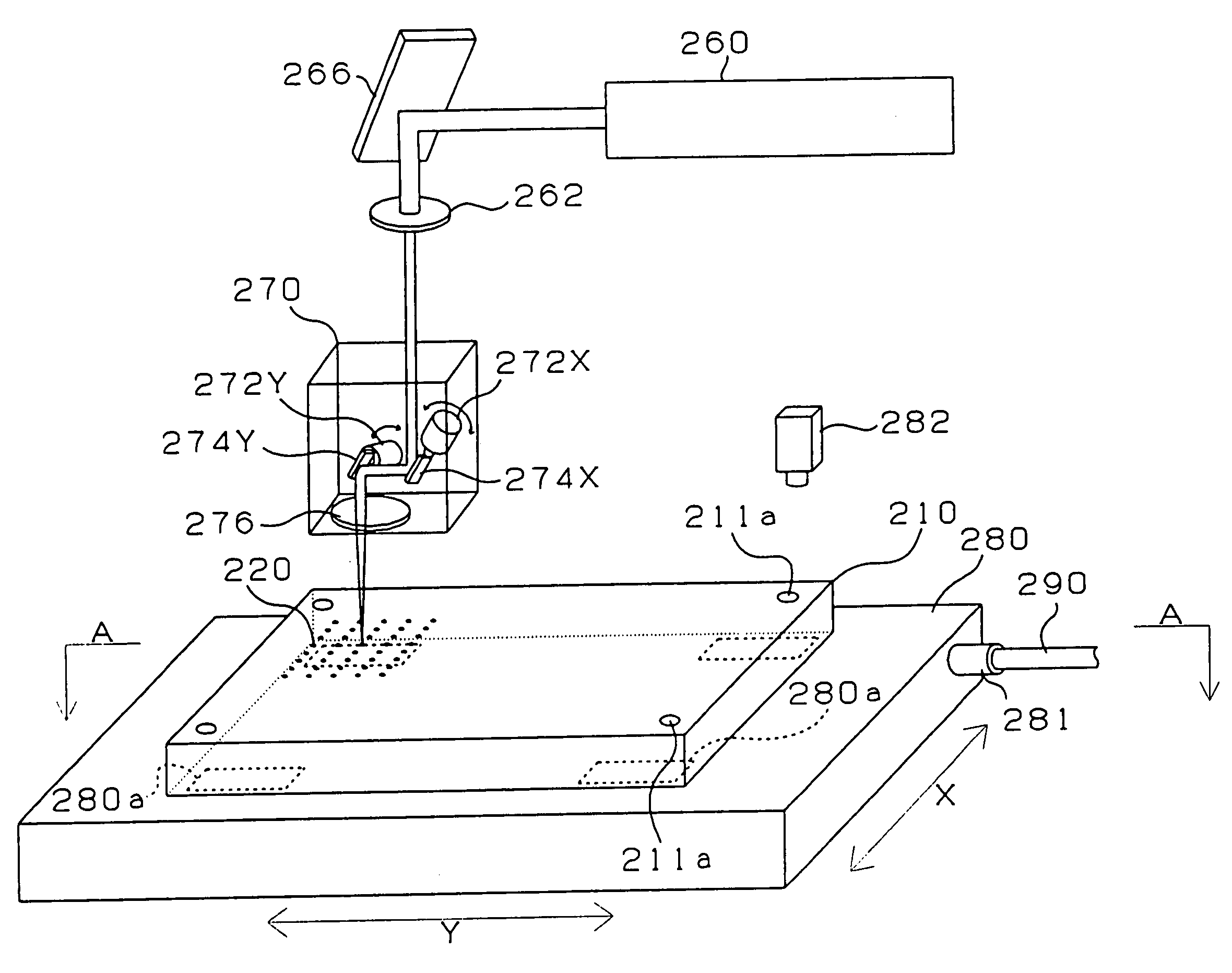
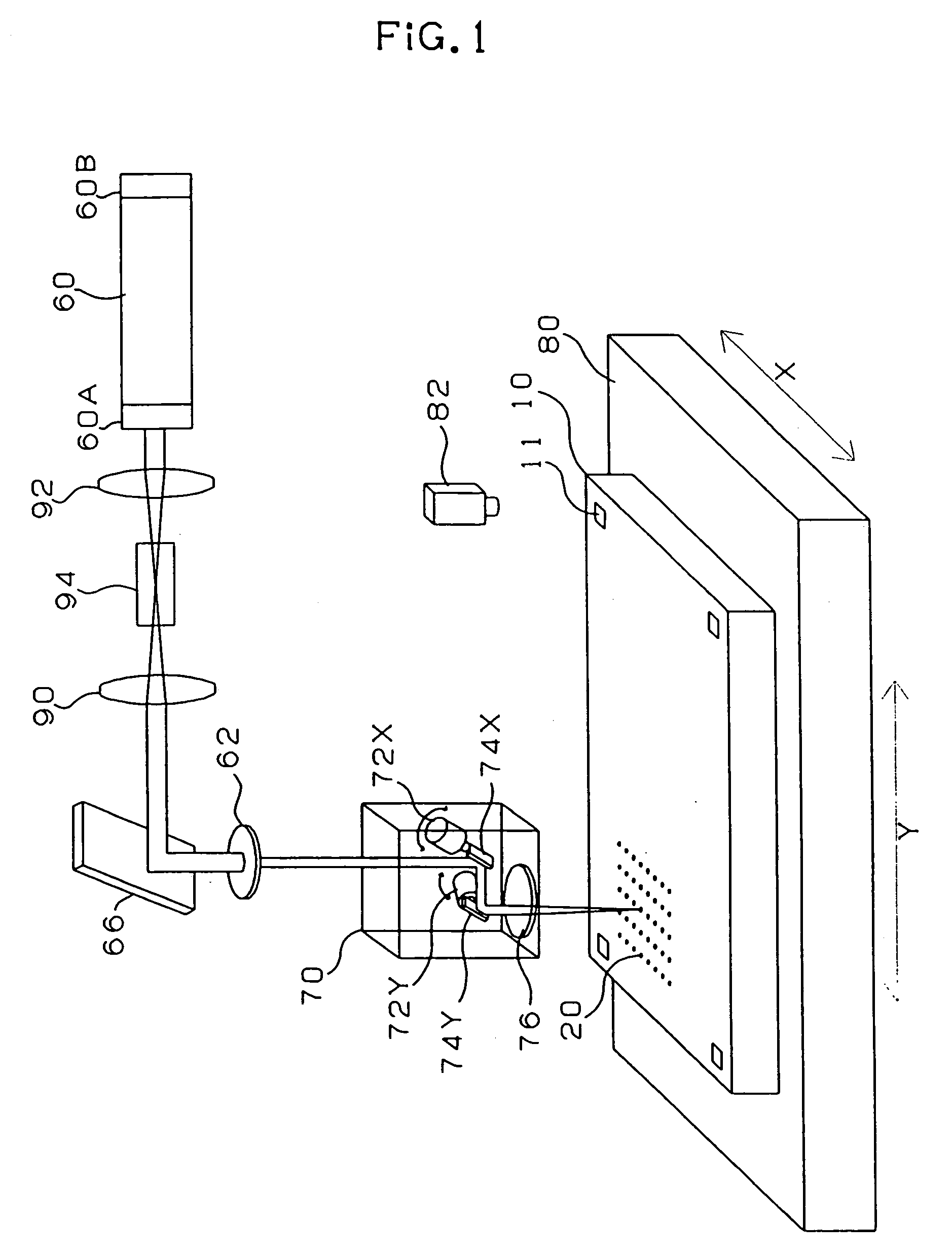
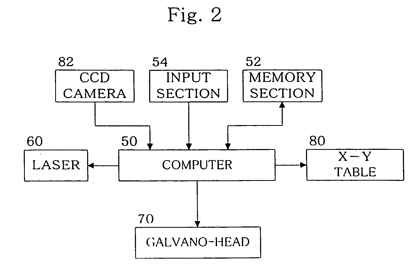
[0132]FIG. 1 shows a multilayer printed wiring board manufacturing apparatus in relation to the an embodiment of the present invention.

[0133] In the embodiment, as the laser source, a CO2 laser oscillator 60 which generates the CO2 laser in the wavelength of 10.6 μm is used. This CO2 laser oscillator 60 is designed as the resonator type oscillator formed by sealing the CO2 gas between a total reflection mirror 60B and a partial reflection mirror 60A. An energy from the excited CO2 is emitted as the laser beam via the partial reflection mirror 60A.

[0134] The laser beam in the beam diameter of 20 mm radiated from the CO2 laser oscillator 60 is condensed by a condenser lens 92 of zinc selenium (ZnSe) coated with a thin film of sodium fluoride (manufactured by MELLES GRIOT) and is then incident to a metal tellurium 94. The surface of the condenser lens 92 is perfectly t...


PUM

PropertyMeasurementUnit
wavelengthaaaaaaaaaa
diameteraaaaaaaaaa

Abstract

There is provided a laser processing apparatus, a multilayer printed wiring board manufacturing apparatus, and a manufacturing method to form via holes of ultra-fine diameter. The laser beam from the CO2 laser oscillator (60) is converted to the shortened wavelength beam by a tellurium crystal (94) to control diffraction of the laser beam. Simultaneously, when the laser beam is condensed, a limit value of the condensation limit is reduced. Thereby, the spot diameter of laser beam is reduced and a hole for via hole is bored on the interlayer insulation resin on a substrate (10). Therefore, even when the laser beam output is raised to form a deeper hole, the hole diameter is not widened and thereby a hole for a small diameter via hole can be formed.

Description

BACKGROUND OF THE INVENTION [0001] 1. Field of the Invention [0002] The present invention relates to a multilayer printed wiring board manufacturing apparatus and method and a laser processing apparatus, particularly to a multilayer printed wiring board manufacturing apparatus and method to form fine holes at a low cost and a laser processing apparatus. [0003] 2. Description of Related Art [0004] A build-up multilayer wiring board alternately has interlayer resin insulators and conductive circuit layers, provides holes to the interlayer resin insulator layers and then electrically connects the upper layers and lower layers by forming conductive films at the wall surface of these holes. [0005] A hole (via hole) of the interlayer resin insulating layer is generally formed through the exposure and developing process by giving photosensitive property to the interlayer resin. [0006] However, the diameter of these via holes on the multilayer printed wiring board is almost 100 μm or less a...

Claims


Application Information

Patent Timeline
01 Dec 2005
Publication
US20050263498A1
IPC
B23K26/04; B23K26/06; B23K26/067; B23K26/08; B23K26/38; H05K1/02; H05K3/00; H05K3/46
CPC
B23K26/032; B23K26/4085; B23K26/06; B23K26/0639; B23K26/0643; B23K26/0648; B23K26/0656; B23K26/0665
Inventors
HIRAMATSU, YASUJI