Stylus system for modifying small structures

Inactive Publication Date: 2005-12-01
FEI COMPANY
View PDF10 Cites 30 Cited by
  • Summary
  • Abstract
  • Description
  • Claims
  • Application Information

AI Technical Summary

Benefits of technology

[0022] The present invention provides a method for rapidly and accurately modifying small structures, including structures on a micron or nanometer scale, and is suitable for the repair of defects in lithographic photo-masks and semiconductors on a nano-scopic level. According to the p

Problems solved by technology

As device density increases, the difficulty of producing photo-masks for the lithographic process without defects also increases.
Defects on photo-mask layers commonly arise from small particles of foreign material, bubbles in the photo-resist, or other flaws introduced during the pattern generation process.
To replace a defective mask is impractical since a subsequently developed mask is as likely to be defective as the mask to be replaced.
For example, although an ideal feature typically has vertical sidewalls, the actual sidewalls may have excessive slope that narrows or widens the feature below its top surface.
However, scans using a greater pixel density take longer to complete and require more resources to store and process.
Cantilever-based AFM instruments suffer from a number of shortcomings that limit their usefulness for mass-production CD metrology applications.
Contact-mode AFMs, especially those where the probe tip remains in constant contact with the sample

Method used


Image

  • Stylus system for modifying small structures
  • Stylus system for modifying small structures
  • Stylus system for modifying small structures

Examples


Embodiment Construction

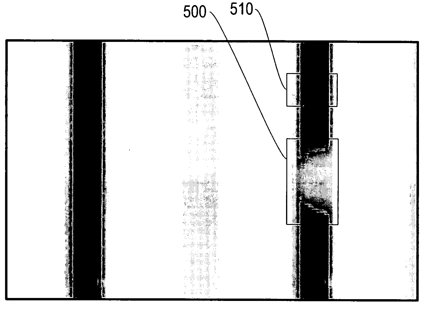
[0034] A preferred embodiment of the present invention provides a method and apparatus for repair of defects in photo masks and semiconductors. In a preferred embodiment, defects within a region of observation are identified. Then, for each defect a “manifold,” that is, a boundary constraint on the region of space through which the probe tip will move to remove material, is defined for repair of the defect. A probe is selected for the repair, which desirably can be the same probe used for observation. The defect is repaired under control of an algorithm and, optionally, the repair region is reexamined and iteration of the repair procedure occurs. These steps are fully automate-able, or the user may be requested to initiate each step sequentially. And the user can select between one programmable sequence of steps and another.

[0035] Thus, in a preliminary step a mask or semiconductor to be repaired is loaded into the instrument of the present invention. The mask / semiconductor (hereaf...


PUM


Abstract

An improved method for rapidly and accurately modifying small structures, including structures on a micron or nanometer scale, suitable for the repair of defects in lithographic photo-masks and semiconductors on a nano-scopic level. Features or samples repaired may be conductive or non-conductive. A single instrument can be employed to both observe the surface of the mask or wafer, and to effectuate the repair of conductive and non-conductive features thereon. Using a Stylus-Nano-Profilometer probe, rapid lateral strokes across the sample surface in a definable pattern at known high applied pressure are used to effectuate defect repair. The tip of the probe can also be dithered rapidly in a pattern or used as to create a jackhammer effect to more effectively remove material from the sample surface.

Description

[0001] This application claims priority from U.S. Prov. Pat. App. 60 / 562,402, filed Apr. 15, 2004, which is hereby incorporated by reference.TECHNICAL FIELD OF THE INVENTION [0002] The present invention relates to the field of repair of mask defects in lithography and repair of defects in semi-conductors. BACKGROUND OF THE INVENTION [0003] Manufacture of semiconductors with high device densities requires the high-resolution lithography of small, closely-spaced features on semiconductor wafers. Such features are typically formed first by a photolithography process in temporary layers of photoresist, and the photoresist features are then used to create permanent structures on the wafer. For example, holes are formed in insulating layers and later filled with a conductive material to create connections between layers in a circuit. Trenches are also formed in insulating layers and later filled with a conductive material to form capacitors. Groups of thin conductive lines are formed to m...

Claims


Application Information

Patent Timeline
IPC IPC(8): B82B3/00G01Q10/00G01Q70/00G01Q80/00G03F1/00H01L21/00H01L21/027
CPCG01Q80/00G03F1/0092B82Y10/00Y10S977/856G03F1/72B82Y40/00G03F1/68
Inventor LINDER, ROBERTKNEEDLER, ERIC
Owner FEI COMPANY
Why Eureka
Try Eureka