Long life-time field emitter for field emission device and method for fabricating the same

a field emission device and long-life technology, which is applied in the manufacture of electric discharge tubes/lamps, discharge tubes with screens, discharge tubes luminescnet screens, etc., can solve the problems of non-uniform length, conductivity and resistance at the lower portions of cnts, and feds' cnt emitters have their own problems, etc., to achieve uniform current density, longer life-time, and higher brightness

Inactive Publication Date: 2005-12-08
SAMSUNG SDI CO LTD
View PDF5 Cites 11 Cited by
  • Summary
  • Abstract
  • Description
  • Claims
  • Application Information

AI Technical Summary

Benefits of technology

[0011] It is still an object of the present invention to provide a carbon nanotube (CNT) emitter for a field emission device (FED) designed to offer more uniform current density, longer life-time, and higher brightness.

Problems solved by technology

However, CNT emitters for FEDs have their own problems.
CNTs are often plagued by non-uniformity in length, conductivity and resistance at lower portions of the CNT.

Method used


Image

  • Long life-time field emitter for field emission device and method for fabricating the same
  • Long life-time field emitter for field emission device and method for fabricating the same
  • Long life-time field emitter for field emission device and method for fabricating the same

Examples


first embodiment

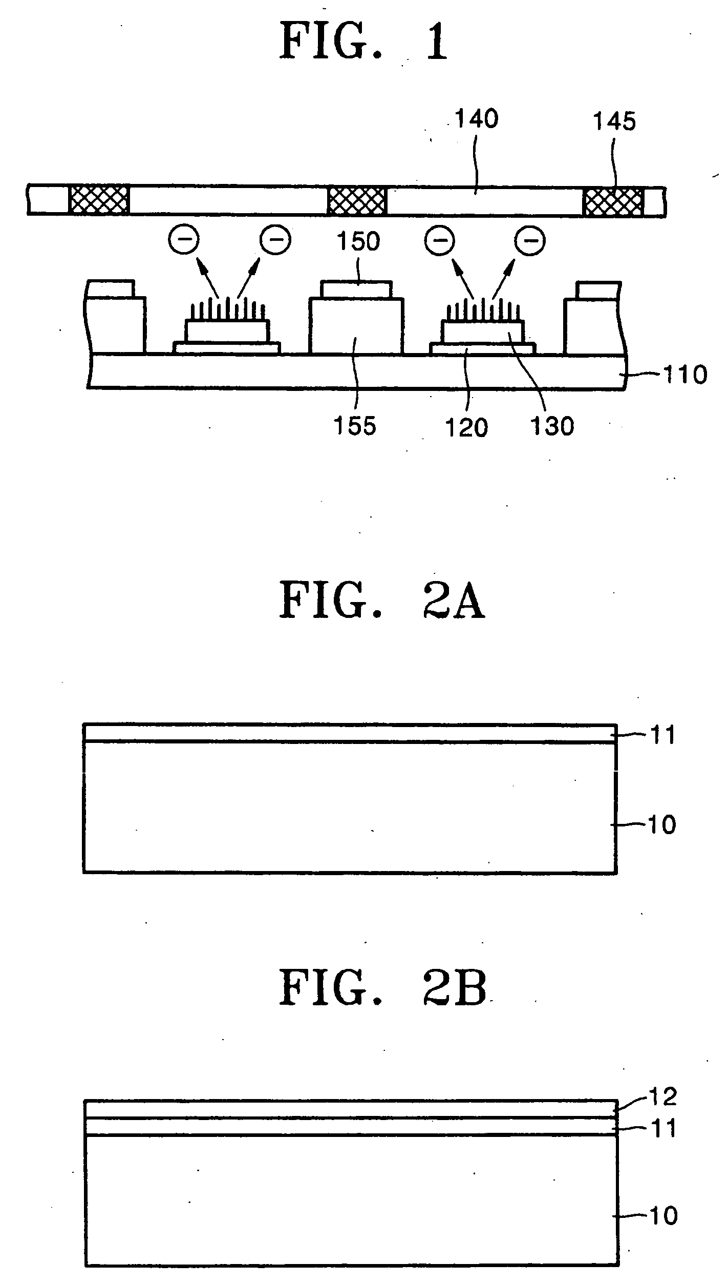
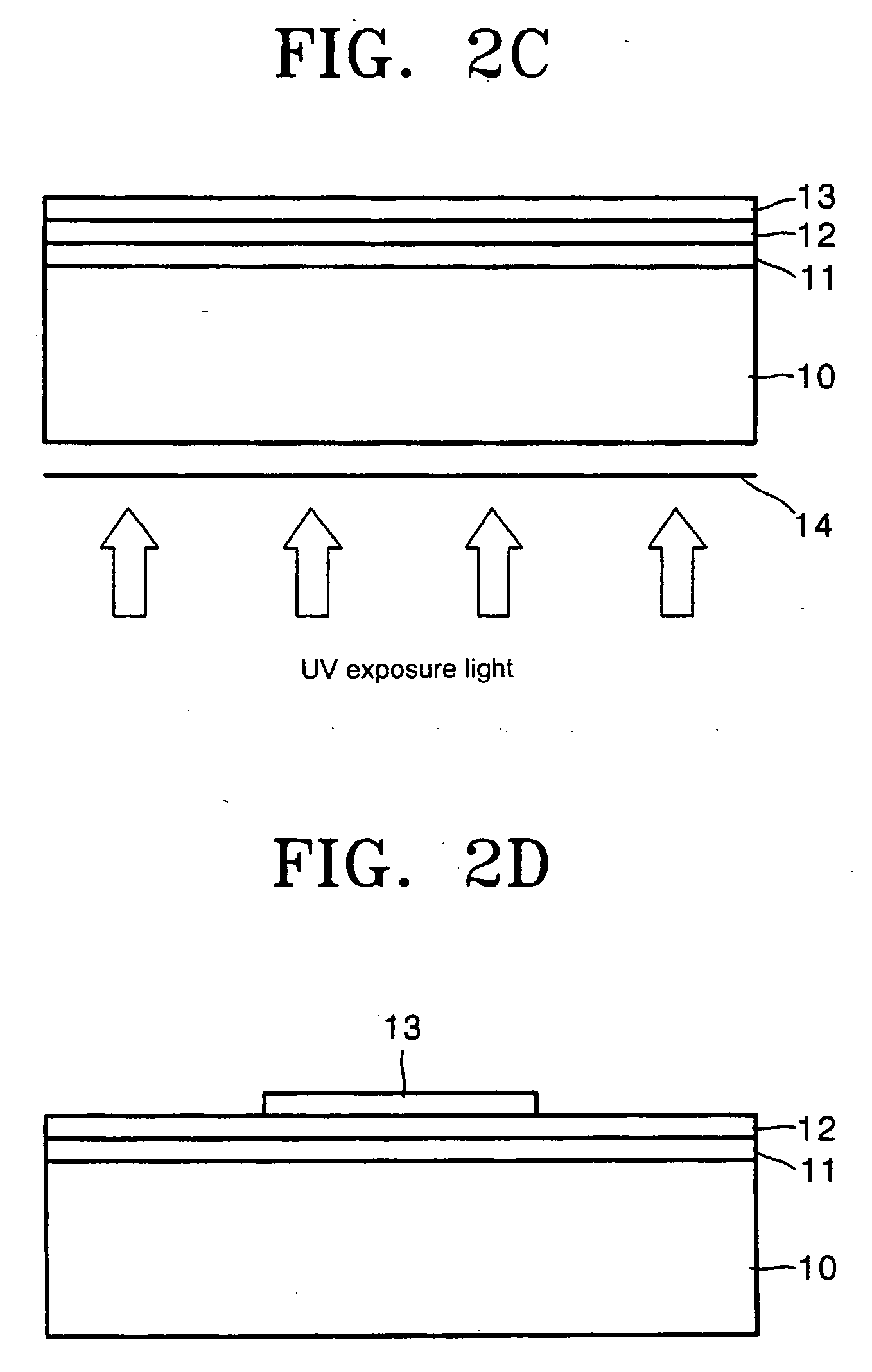
[0030] Turning now to FIGS. 2A through 2E, FIGS. 2A through 2E illustrate a method of making a diode-type FED according to the present invention. Referring to FIG. 2A, a transparent electrode 11 such as indium tin oxide (ITO) is first deposited over a transparent substrate 10 such as glass. Turning now to FIG. 2B, a resistive layer 12 is then formed on the transparent electrode 11. The resistive layer 12 is used to provide a uniform current to the CNT. Instead of using non-UV transmissive amorphous silicon (a-Si) for the resistive layer, an ultraviolet (UV) transmissive resistive material is used in the present invention to allow for a patterning process using back exposure. The resistive material has a resistivity greater than 10 Ω·m, and is preferably in the range of 102 Ω·m to 103 Ω·m, in order to obtain a sufficient voltage drop. Examples of the material satisfying these requirements for the resistive layer 12 include Cr2O3, Na2O2, SO2, CaO, Sc2O3, TiO2, VO2, V2O5, Mn3O4, Fe2O3,...

second embodiment

[0036] Turning now to FIGS. 3A through 3G, FIGS. 3A-3G are cross-sectional views illustrating a method of fabricating an emitter for a triode-type FED according to the present invention. Unlike the diode-type FED of FIGS. 2A through 2E, the triode-type FED includes a gate electrode.

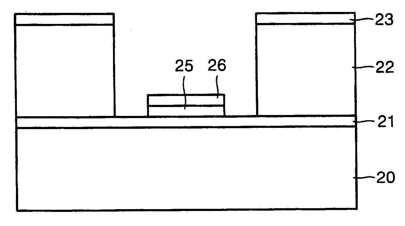
[0037] Turning now to FIG. 3A, a transparent electrode 21 preferably made of ITO is deposited on a transparent substrate 20 preferably made of glass. Turning now to FIG. 3B, insulating layers 22 are formed at opposite ends of the top surface of the transparent electrode 21. A middle portion of the top surface of the transparent electrode 21 between the insulating layers 22 is reserved to form a resistive layer and an emitter layer during a subsequent processes. The insulating layers 22 are formed by applying a paste containing an insulating material such as SiO2 or PbO on the transparent electrode 21 and then solidifying the same through a sintering process. Subsequently, as illustrated in FIG. 3C, a cond...


PUM


Abstract

An emitter for a field emission device (FED) designed to increase durability by interposing an ultraviolet (UV) transmissive resistive layer between a substrate and an emitter and a method for fabricating the same. The method includes depositing a transparent electrode on a transparent substrate, forming a resistive layer by stacking an ultraviolet (UV) transmissive resistive material on the transparent electrode, forming an emitter layer by stacking a carbon nanotube (CNT) on the UV transmissive resistive material, and patterning the emitter layer according to a predetermined emitter pattern.

Description

CLAIM OF PRIORITY [0001] This application makes reference to, incorporates the same herein, and claims all benefits accruing under 35 U.S.C. §119 from an application entitled LONG LIFE-TIME FIELD EMITTER FOR FIELD EMISSION DEVICE AND METHOD FOR FABRICATING THE SAME filed with the Korean Industrial Property Office on Jun. 3, 2004 and there duly assigned Serial No. 10-2004-0040313. BACKGROUND OF THE INVENTION [0002] 1. Field of the Invention [0003] The present invention relates to a durable emitter for a field emission device (FED), and a method for fabricating the same, and more particularly, to an emitter for a FED designed to increase the life span by interposing an ultraviolet (UV) transmissive resistive layer between a substrate and an emitter and a method for fabricating the same. [0004] 2. Description of the Related Art [0005] As display technology advances, a flat panel displays are becoming more widely used than traditional cathode ray tube (CRT) displays. A representative ex...

Claims


Application Information

Patent Timeline
Patent Type & Authority Applications(United States)
IPC IPC(8): H01J31/12H01J1/00H01J1/14H01J1/304H01J9/02H01J9/04
CPCB82Y10/00H01J2201/30469H01J9/025H01J1/3048C01B32/158B82Y40/00C01B2202/06C01B2202/02
Inventor KIM, WON-SEOKHA, JAE-SANGLEE, JEONG-HEEJEONG, TAE-WONKONG, BYUNG-YUN
Owner SAMSUNG SDI CO LTD
Why Eureka
Try Eureka