

Infrared detection element, infrared detector, solid state imaging device, and method for fabricating infrared detector
- Summary
- Abstract
- Description
- Claims
- Application Information
AI Technical Summary
Benefits of technology
Problems solved by technology
Method used
Image

Examples
first embodiment
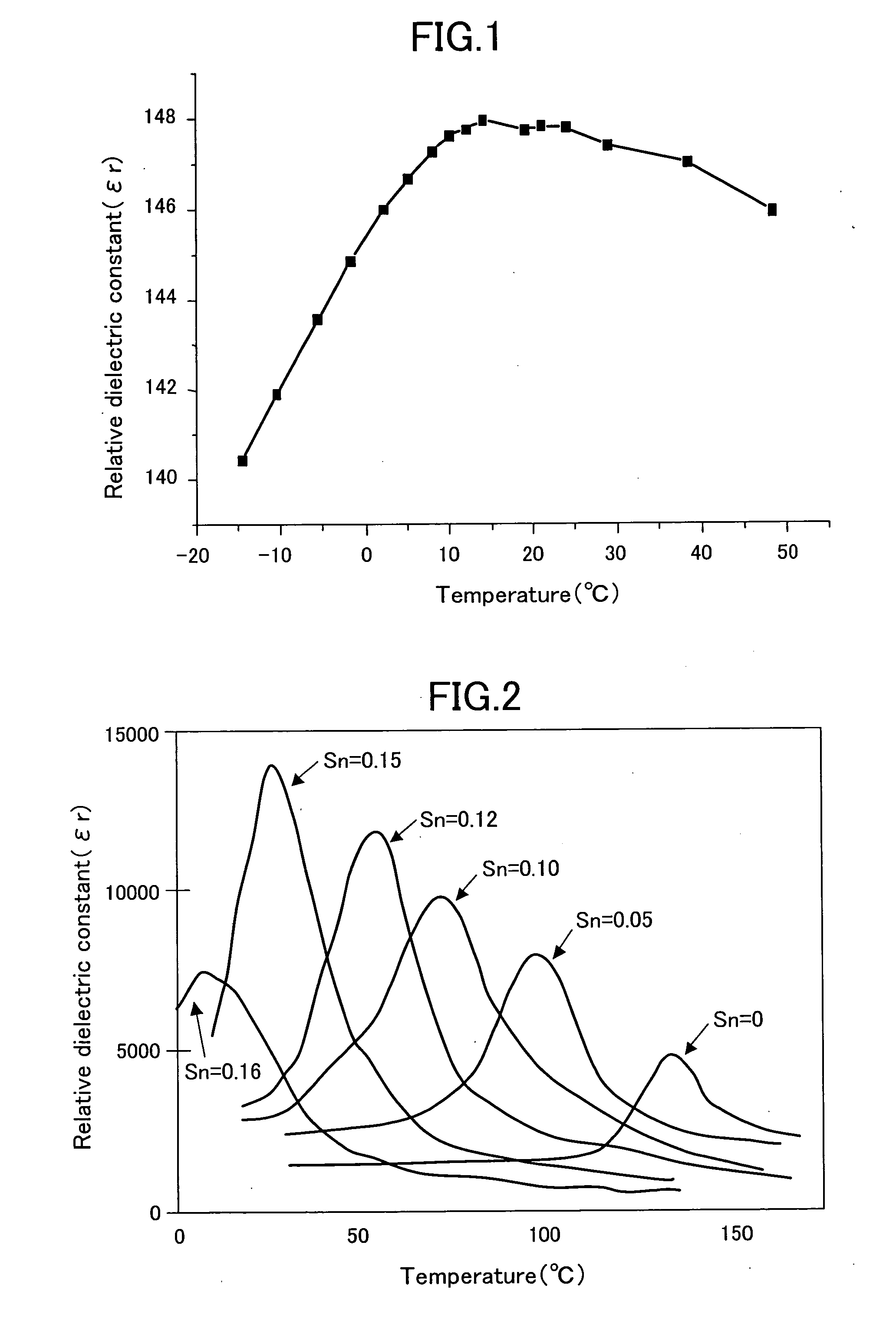
[0048] An infrared detection film (infrared detection element) according to a first embodiment of the present invention is a material of which a relative dielectric constant is changed due to change in temperature caused by incident infrared light and is also a dielectric bolometer oxide thin film expressed by a chemical formula of Ba(Ti1-xSnx)O3 (01-xSnx)O3 (03 with tin atoms and the Sn composition ratio x in BTS is not less than 0.1 and not more than 0.2. Specifically, the infrared detection film of this embodiment is, for example, a dielectric film of Ba(Ti1-xSnx)O3 (0.10≧x≧0.20) formed on a lower electrode made of platinum (Pt) formed over a silicon substrate, and having a thickness of 2 μm or less. An absolute value of temperature coefficient of dielectric (TCD) is 2% or more. TCD indicates the rate of change in relative dielectric constant according to temperature change for the infrared detection film of this embodiment as a phase transition from a ferroelectric to a paraelec...
second embodiment
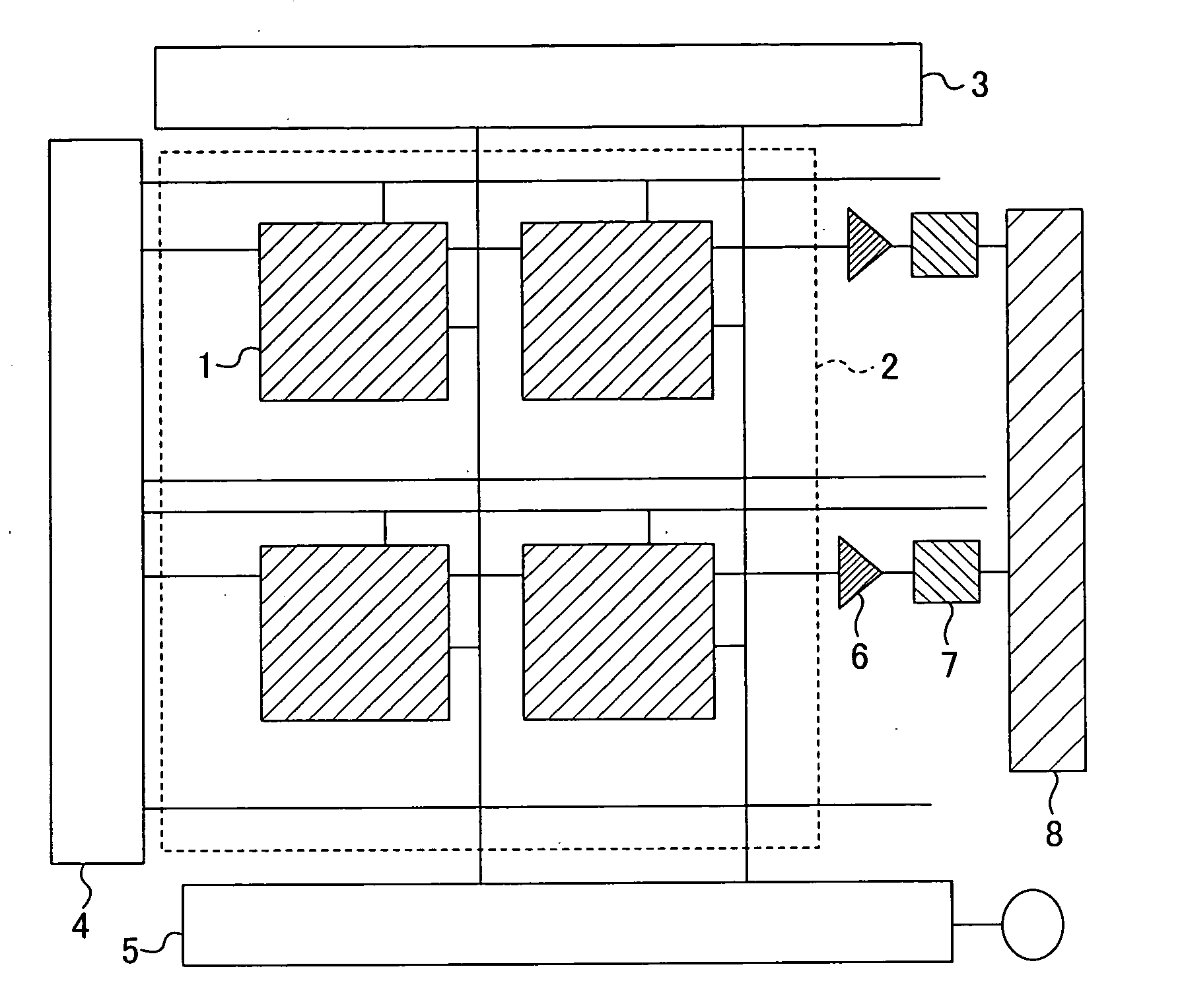
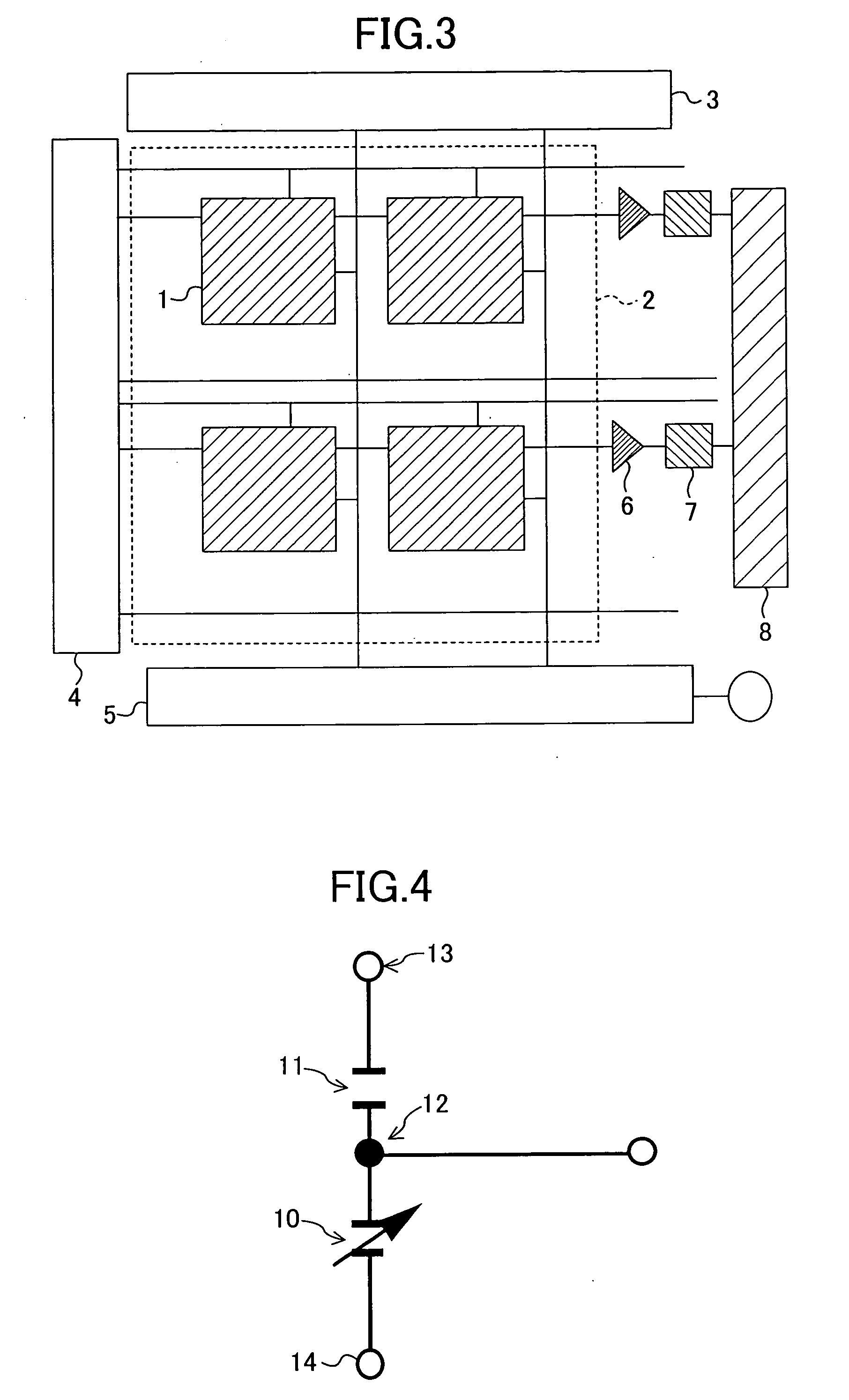
[0057] As a second embodiment of the present invention, a solid state imaging device including a dielectric bolometer having the infrared detection film of the first embodiment which is formed of Ba(Ti1-xSnx)O3 (0<x<1) will be described. The solid state imaging device of this embodiment is a dielectric bolometer thermal infrared imaging device which reads out change in a relative dielectric constant of a material according to temperature change due to incident infrared radiation as a signal indicating the intensity of the incident infrared radiation. Moreover, the solid state imaging device of this embodiment is characterized by including unit pixels each having the infrared detection film of the first embodiment, and having a structure in which the unit pixels are arranged in the one- or two-dimensional manner.
[0058]FIG. 3 is a diagram illustrating an exemplary configuration of the dielectric bolometer thermal infrared solid state imaging device of this embodiment.
[0059] As shown...
third embodiment
[0066] As a third embodiment of the present invention, a method for fabricating an infrared detection film (a dielectric bolometer thin film, i.e., an infrared detection element) in a composition expressed by Ba(Ti1-xSnx)O3 (0<x<1) will be described. In the method of this embodiment, a BTS film is formed using metal organic decomposition (MOD). MOD has mainly the following four advantages: (1) accurate stoichiometry control can be performed; (2) excellent uniformity in film formation can be achieved; (3) MOD is suitable for formation of a film with a large area; and (4) fabrication device and method are low-cost and very simple. Because of the four advantages described above, MOD can be adopted to a method for fabricating a BTS film, so that a BTS thin film having a large TCD can be formed at low cost and in a relatively simple manner.
[0067]FIG. 5 is a flow chart showing respective steps for fabricating a BTS film using MOD.
[0068] Normal MOD includes mainly four different process ...
PUM
 Abstract
Description
Claims
Application Information