Semiconductor laser device and method for fabricating the same

a laser device and semiconductor technology, applied in the direction of semiconductor lasers, lasers, solid-state devices, etc., can solve the problems of reducing reliability of semiconductor laser devices using nitride materials, increasing the absorption of emitted light, and deteriorating device characteristics, so as to improve the crystallinity and surface morphology of semiconductor layers

Active Publication Date: 2005-12-22
PANASONIC CORP
View PDF7 Cites 8 Cited by
  • Summary
  • Abstract
  • Description
  • Claims
  • Application Information

AI Technical Summary

Benefits of technology

[0015] The present invention has been made to solve the aforementioned problems, and an object of the present invention is to improve the crystallinity and surface morphology of a semiconductor layer formed on a current blocking layer and realize a high-reliability semiconductor laser device with a small lasing threshold current.

Problems solved by technology

If the recess is formed by dry etching, part of the current blocking layer 108 subjected to dry etching, such as an exposed part of the p-type guide layer 106, is damaged, resulting in the increased absorption of emitted light and the deteriorated device characteristics.
However, the buried heterostructure semiconductor laser device has the following problems.
When Mg has diffused into the active region 105, a semiconductor laser device using a nitride material has reduced reliability.

Method used


Image

  • Semiconductor laser device and method for fabricating the same
  • Semiconductor laser device and method for fabricating the same
  • Semiconductor laser device and method for fabricating the same

Examples


Embodiment Construction

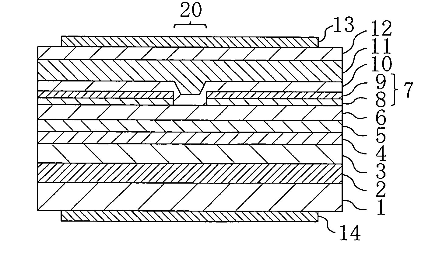
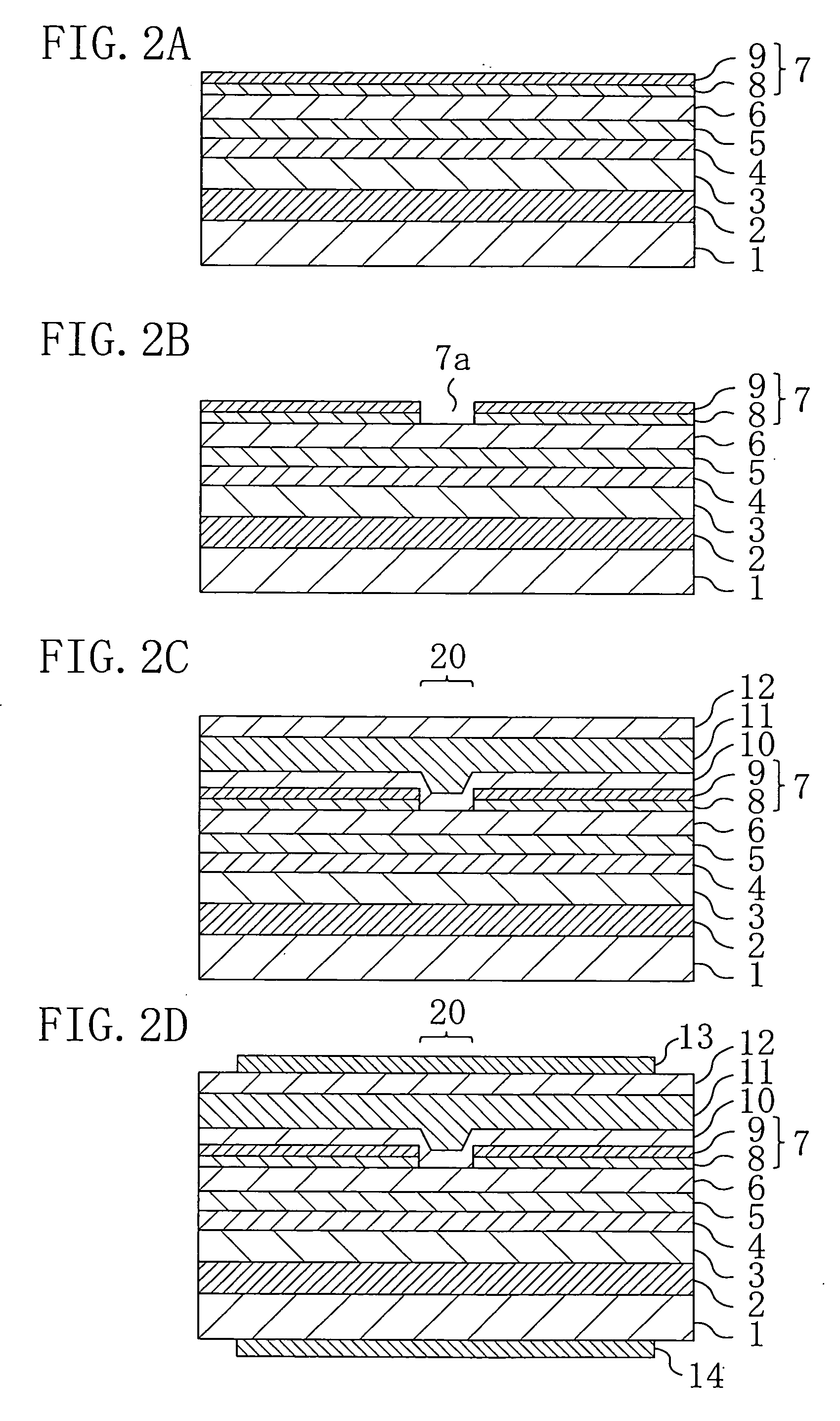
[0037] A semiconductor laser device according to a first embodiment of the present invention will be described with reference to the drawings. FIG. 1 shows a cross-sectional structure of the semiconductor laser device according to the first embodiment. As shown in FIG. 1, an n-type GaN layer 2 is formed on a 2-inch substrate 1 made of GaN. The following layers are successively stacked on the GaN layer 2: an n-type cladding layer 3 of n-type Al0.06Ga0.94N; an n-type guide layer 4 of n-type GaN; an active layer 5 of InGaN having a multi-quantum well structure; and a first p-type guide layer 6 of p-type GaN.

[0038] A current blocking layer 7 is formed on the first p-type guide layer 6 to have a groove obtained by etching a part of the current blocking layer 7 in a stripe. The current blocking layer 7 is obtained by successively stacking an n-type Al0.15Ga0.85N layer 8 and an n-type GaN layer 9. A second p-type guide layer 10 of p-type GaN is formed on a part of the first p-type guide l...


PUM


Abstract

A semiconductor laser device of the present invention includes: an active layer formed on a substrate; a first semiconductor layer formed on the active layer and made of a nitride semiconductor of a first conductivity type; a multilayer film formed on the first semiconductor layer and having a groove; and a second semiconductor layer formed on the multilayer film to fill the groove and made of a nitride semiconductor of the first conductivity type. The multilayer film is composed of a plurality of thin films containing a nitride semiconductor of a second conductivity type, and one of the thin films formed as the uppermost film is made of gallium nitride.

Description

CROSS-REFERENCE TO RELATED APPLICATIONS [0001] This application claims priority under 35 U.S.C. §119 on Patent Application No. 2004-179264 filed in Japan on Jun. 17, 2004, the entire contents of which are hereby incorporated by reference. The entire contents of Patent Application No. 2005-172841 filed in Japan on Jun. 13, 2005 are also incorporated by reference. BACKGROUND OF THE INVENTION [0002] (1) Field of the Invention [0003] The present invention relates to a semiconductor laser device using a nitride semiconductor and a method for fabricating the same. [0004] (2) Description of Related Art [0005] Laser diodes emitting in the blue-violet region of the spectrum are expected as light sources for high-density optical disks, because the diameter of the focused laser spot on the optical disks can be reduced as compared with light diodes emitting in the red and infrared regions and therefore can improve the recording density for the optical disks. Semiconductor laser devices using ni...

Claims


Application Information

Patent Timeline
Patent Type & Authority Applications(United States)
IPC IPC(8): H01L29/06H01S5/20H01S5/22H01S5/343
CPCB82Y20/00H01S5/2081H01S5/34333H01S5/222H01S5/2202H01L2224/48091H01L2924/00014
Inventor TAMURA, SATOSHIIKEDO, NORIO
Owner PANASONIC CORP
Why Eureka
Try Eureka