High density bonding of electrical devices

a high density, electrical device technology, applied in the direction of basic electric elements, electrical apparatus, semiconductor devices, etc., can solve the problems of large area reducing the accuracy required for placement of ics during manufacture, serious limitations of high-speed manufacturing, and conventional thermocompression bonding devices

Inactive Publication Date: 2005-12-22
AVERY DENNISON CORP
View PDF22 Cites 50 Cited by
  • Summary
  • Abstract
  • Description
  • Claims
  • Application Information

AI Technical Summary

Problems solved by technology

Pick and place techniques typically involve complex robotic components and control systems that handle only one die at a time.
The larger area reduces the accuracy required for placement of ICs during manufacture while still providing effective electrical connection.
IC placement and mounting are serious limitations for high-speed manufacture.
However, conventional thermocompression bonding devices have several disadvantages.
For example, conventional thermocompression bonding devices are not well suited for applying uniform heat and uniform pressure simultaneously to many chips and/or to a very dense web of electri

Method used


Image

  • High density bonding of electrical devices
  • High density bonding of electrical devices
  • High density bonding of electrical devices

Examples


Embodiment Construction

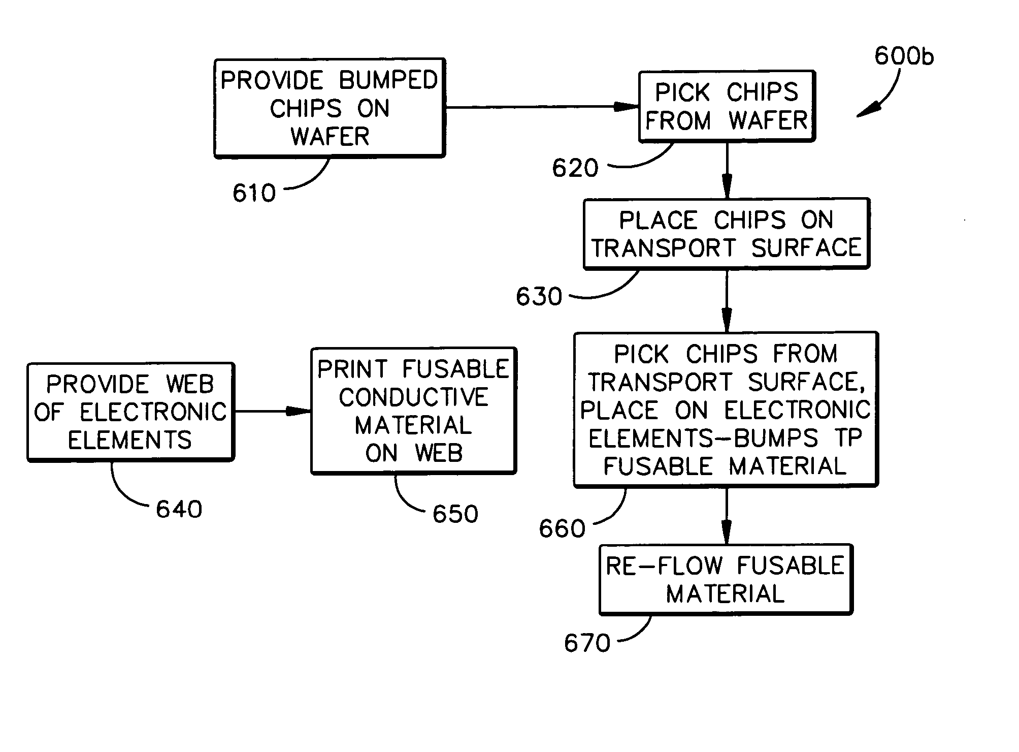
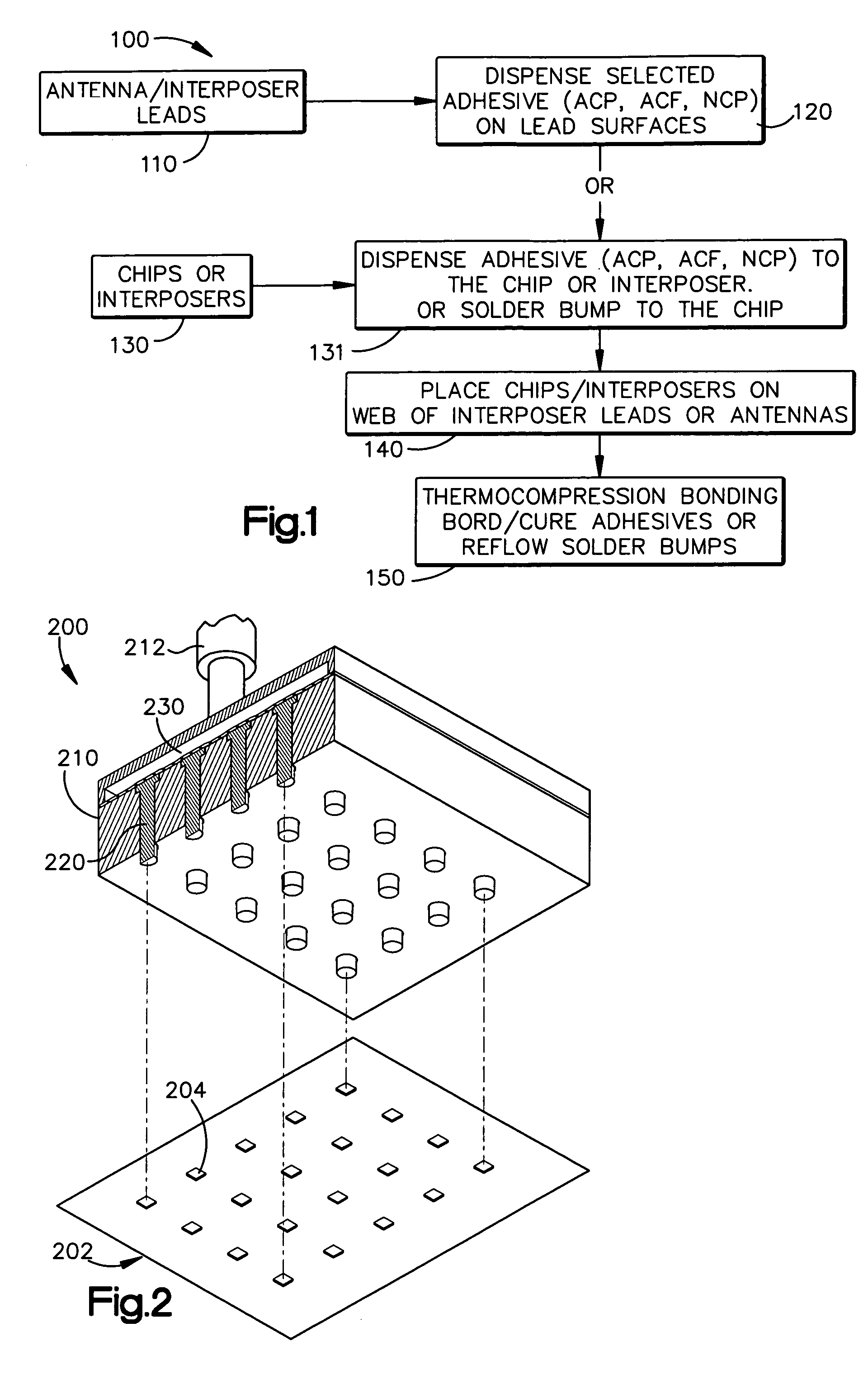
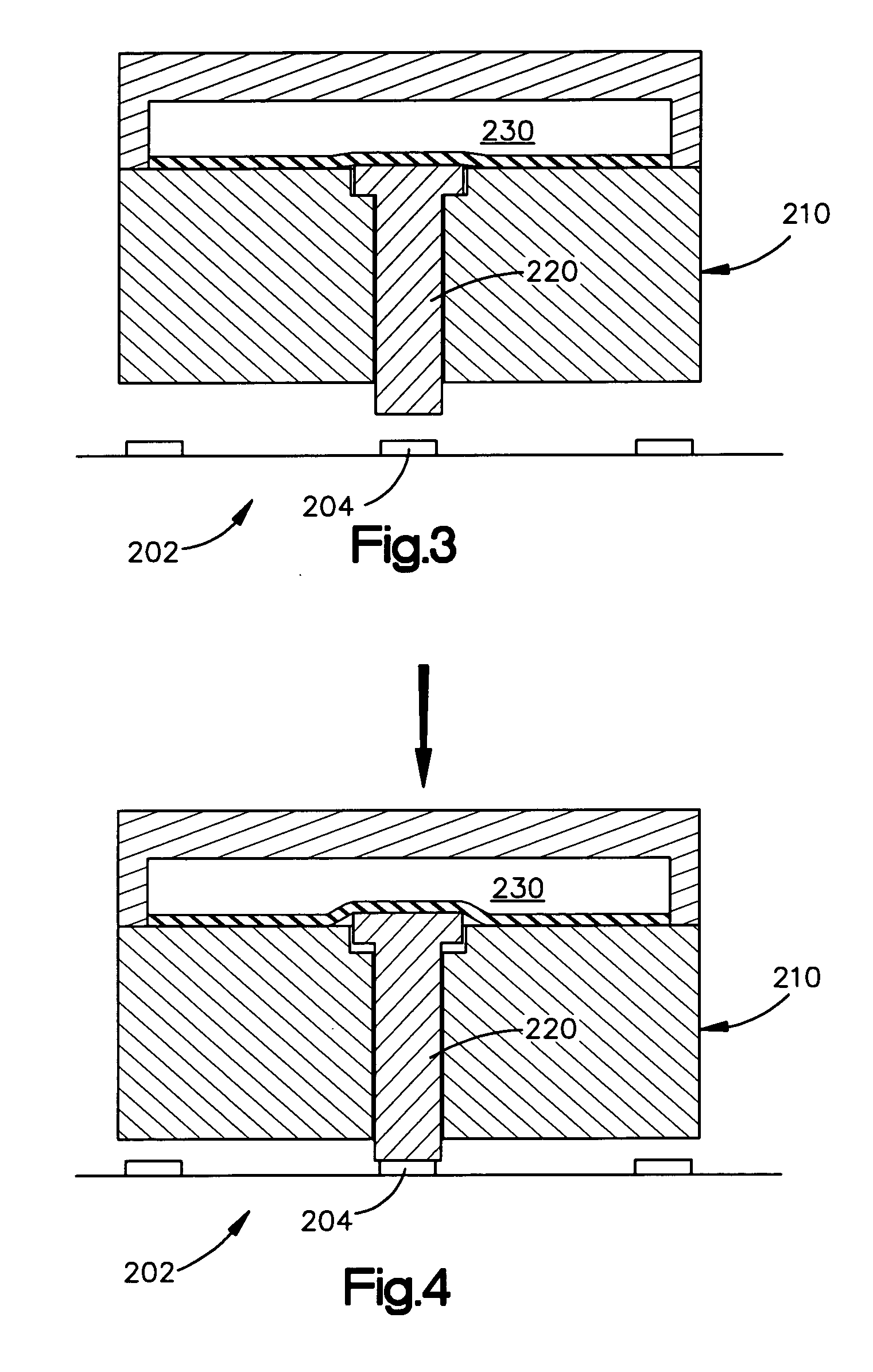
[0039] A method of simultaneous thermocompressive bonding of multiple electrical devices using individual heating elements and a resilient member to force the individual heating elements into compressive engagement with the electrical devices is provided. The individual heating elements may be Curie-point heating elements or conventional resistive heating elements. A method of simultaneous thermocompressive bonding of multiple electrical devices using a transparent flexible platen and thermal radiation is also provided. In one embodiment, the thermal radiation is near infra-red thermal radiation and the transparent flexible platen is composed of silicone rubber. The bonding material may be an adhesive or a thermoplastic bonding material. A method of capacitively coupling a semiconductor chip to an electrical component with a pressure sensitive adhesive is also provided. The method includes compressing the chip by forcing a flexible platen of a bonding device into compressive engagem...


PUM


Abstract

A method of thermocompressive bonding of one or more electrical devices using individual heating elements and a resilient member to force the individual heating elements into compressive engagement with the electrical devices is provided. The individual heating elements may be Curie-point heating elements or conventional resistive heating elements. A method of thermocompressive bonding of one or more electrical devices using a transparent flexible platen and thermal radiation is also provided. In one embodiment, the thermal radiation is near infra-red thermal radiation and the transparent flexible platen is composed of silicone rubber. The bonding material may be an adhesive or a thermoplastic bonding material. A method of capacitively coupling a semiconductor chip to an electrical component with a pressure sensitive adhesive is also provided. The method includes compressing the chip by forcing a flexible platen of a bonding device into compressive engagement with the semiconductor chip.

Description

BACKGROUND OF THE INVENTION [0001] 1. Field of the Invention [0002] The present invention relates generally to the assembly of electrical devices. More particularly, the present invention relates to the assembly of radio frequency identification (RFID) straps and / or tags. [0003] 2. Description of the Related Art [0004] Pick and place techniques are often used to assemble electrical devices. Pick and place techniques typically involve complex robotic components and control systems that handle only one die at a time. Such techniques typically involve a manipulator, such as a robotic arm, to remove integrated circuit (IC) chips, or dies, from a wafer of IC chips and place them on a chip carrier or transport or directly to a substrate. If not directly mounted, the chips are subsequently mounted onto a substrate with other electrical components, such as antennas, capacitors, resistors, and inductors to form an electrical device. [0005] One type of electrical device that may be assembled ...

Claims


Application Information

Patent Timeline
IPC IPC(8): H01L21/30H01L21/44H01L21/46H01L21/48H01L21/50H01L21/60H01L21/603
CPCH01L24/75H01L24/81H01L2924/07802H01L2924/10253H01L2924/014H01L2224/16H01L2224/75315H01L2224/81801H01L2924/01029H01L2924/01033H01L2924/01047H01L2924/01078H01L2924/01082H01L2924/14H01L2924/19041H01L2924/19042H01L2924/19043H01L2924/30105H01L2924/3011H01L2924/01019H01L2924/01075H01L2924/00
Inventor EDWARDS, DAVID N.MUNN, JASONKIAN, KOUROCHEMEHRABI, REZAFORSTER, IAN J.WEAKLEY, THOMAS CRAIG
Owner AVERY DENNISON CORP
Why Eureka
Try Eureka