Systems and methods for forming metal oxides using metal organo-amines and metal organo-oxides

a technology of metal organoamines and metal oxides, which is applied in the direction of coatings, transistors, chemical vapor deposition coatings, etc., can solve the problems of forming an undesirable siosub>2 /sub>interfacial layer, the traditional use of integrated circuit technology is approaching its performance limits, and the layer no longer effectively functions as an insulator

a technology of metal organoamines and metal oxides, which is applied in the direction of coatings, transistors, chemical vapor deposition coatings, etc., can solve the problems of forming an undesirable siosub>2 /sub>interfacial layer, the traditional use of integrated circuit technology is approaching its performance limits, and the layer no longer effectively functions as an insulator

US20050287819A1Inactive Publication Date: 2005-12-29MICRON TECH INC

Image

  • Systems and methods for forming metal oxides using metal organo-amines and metal organo-oxides
  • Systems and methods for forming metal oxides using metal organo-amines and metal organo-oxides
  • Systems and methods for forming metal oxides using metal organo-amines and metal organo-oxides

Examples


example

Example 1

Atomic Layer Deposition of (Hf,Ti)O2

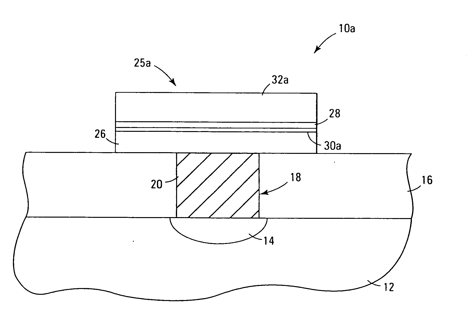
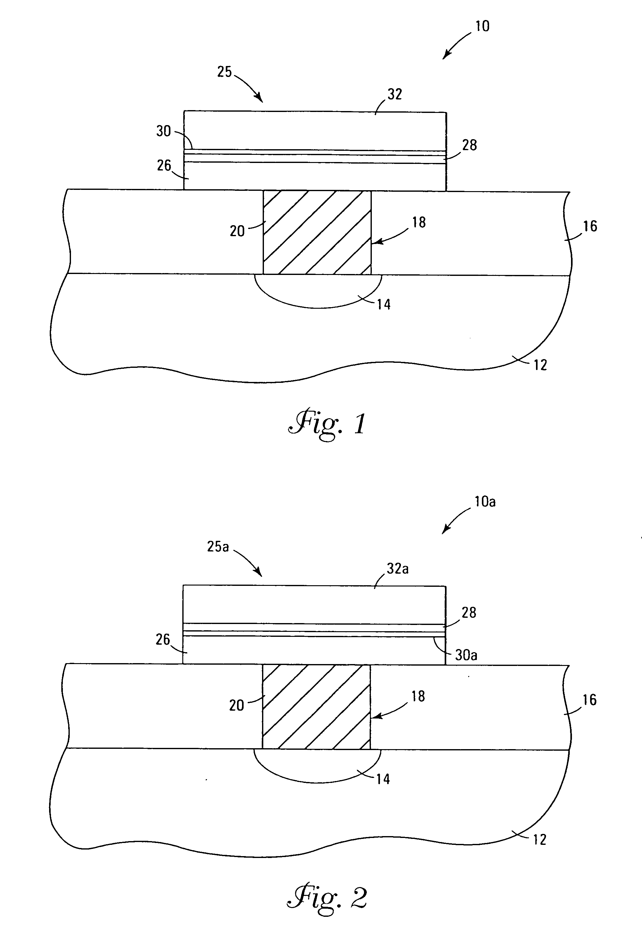
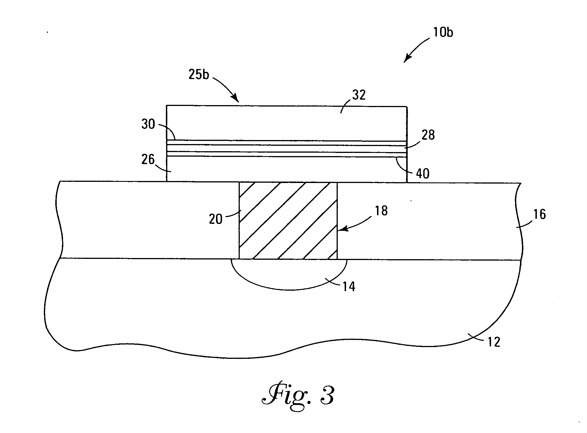
[0071] A chamber of configuration shown in FIG. 4 was set up with pneumatic valves under computer control to pulse the valves open in sequential manner. Two reservoirs connected to the chamber contained Ti(NMe2)4 and Hf(OC(CH3)3)4 (Strem Chemical, Newburyport, Mass.). The substrate was a silicon wafer having doped poly-silicon as a top layer and was maintained at 150° C. for the deposition.

[0072] Each cycle involved a 5-second pulse of Hf(OC(CH3)3)4 and a 5-second pulse of Ti(NMe2)4, each separated by a 10-second purge with argon and a 20-second pump down under dynamic vacuum. The precursors were introduced with helium carrier gas, using mass flow controllers set at 5 sccm. After 400 cycles a (Hf,Ti)O2 film 180 â„« thick was obtained. The film was nearly 50 / 50 Hf / Ti based on x-ray photoelectron spectroscopy (XPS) analysis, and had no detectable nitrogen or carbon.


PUM

PropertyMeasurementUnit
temperatureaaaaaaaaaa
pressureaaaaaaaaaa
thicknessaaaaaaaaaa

Abstract

A method of forming (and an apparatus for forming) a metal oxide layer on a substrate, particularly a semiconductor substrate or substrate assembly, using a vapor deposit ion process and one or more precursor compounds that include organo-amine ligands and one or more precursor compounds that include organo-oxide ligands.

Description

FIELD OF THE INVENTION [0001] This invention relates to methods of forming a metal oxide layer on a substrate using one or more precursor compounds that include one or more organo-amine precursor compounds (e.g., alkylamine or alkylimino-alkylamine precursor compounds) with one or more organo-oxide precursor compounds (e.g., alkoxide or oxo-alkoxide) precursor compounds during a vapor deposition process. The precursor compounds and methods are particularly suitable for the formation of a metal oxide layers on semiconductor substrates or substrate assemblies. BACKGROUND OF THE INVENTION [0002] The continuous shrinkage of microelectronic devices such as capacitors and gates over the years has led to a situation where the materials traditionally used in integrated circuit technology are approaching their performance limits. Silicon (i.e., doped polysilicon) has generally been the substrate of choice, and silicon dioxide (SiO2) has frequently been used as the dielectric material with si...

Claims


Application Information

Patent Timeline
29 Dec 2005
Publication
US20050287819A1
IPC
C23C16/40; C23C16/44; C23C16/455; H01L21/316; H01L21/822; H01L21/8242; H01L21/8244; H01L21/8246; H01L27/04; H01L27/105; H01L27/108; H01L27/11; H01L29/78
CPC
C23C16/405; H01L21/31604; C23C16/45553; C23C16/45531; H01L21/02194; H01L21/02175; H01L21/02205; H01L21/02271
Inventors
VAARTSTRA, BRIAN A.; WESTMORELAND, DONALD L.