Plasma processing method and apparatus

a technology of plasma processing and apparatus, applied in the field of plasma processing technique, can solve the problems of difficult to improve the uniformity of process state or process, and difficulty in performing a predetermined plasma process on the substra

Inactive Publication Date: 2006-01-05
TOKYO ELECTRON LTD
View PDF13 Cites 56 Cited by
  • Summary
  • Abstract
  • Description
  • Claims
  • Application Information

AI Technical Summary

Benefits of technology

[0010] An object of the present invention is to provide a plasma processing apparatus and method, which can optimize a plasma process in which radicals and ions act on a target substrate at the same time.

Problems solved by technology

However, if radicals and ions are always limited or restricted to such a relationship that they have the same distribution in acting on the substrate surface, it is difficult to perform a predetermined plasma process on the substrate, and it is particularly difficult to improve the uniformity in process state or process result.

Method used


Image

  • Plasma processing method and apparatus
  • Plasma processing method and apparatus
  • Plasma processing method and apparatus

Examples


first embodiment

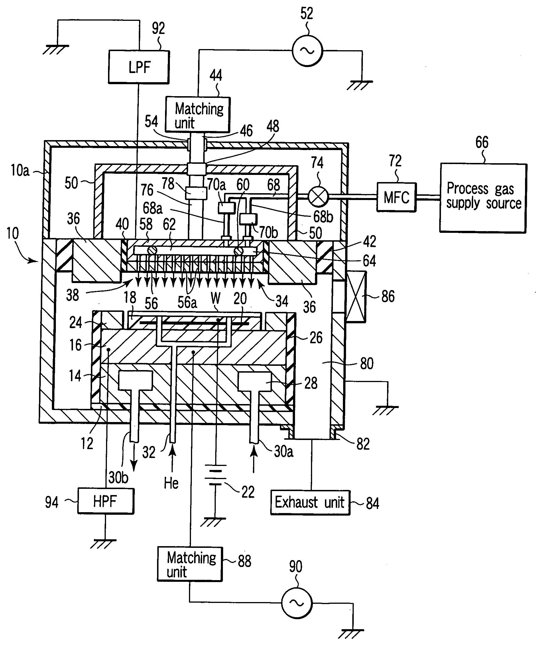
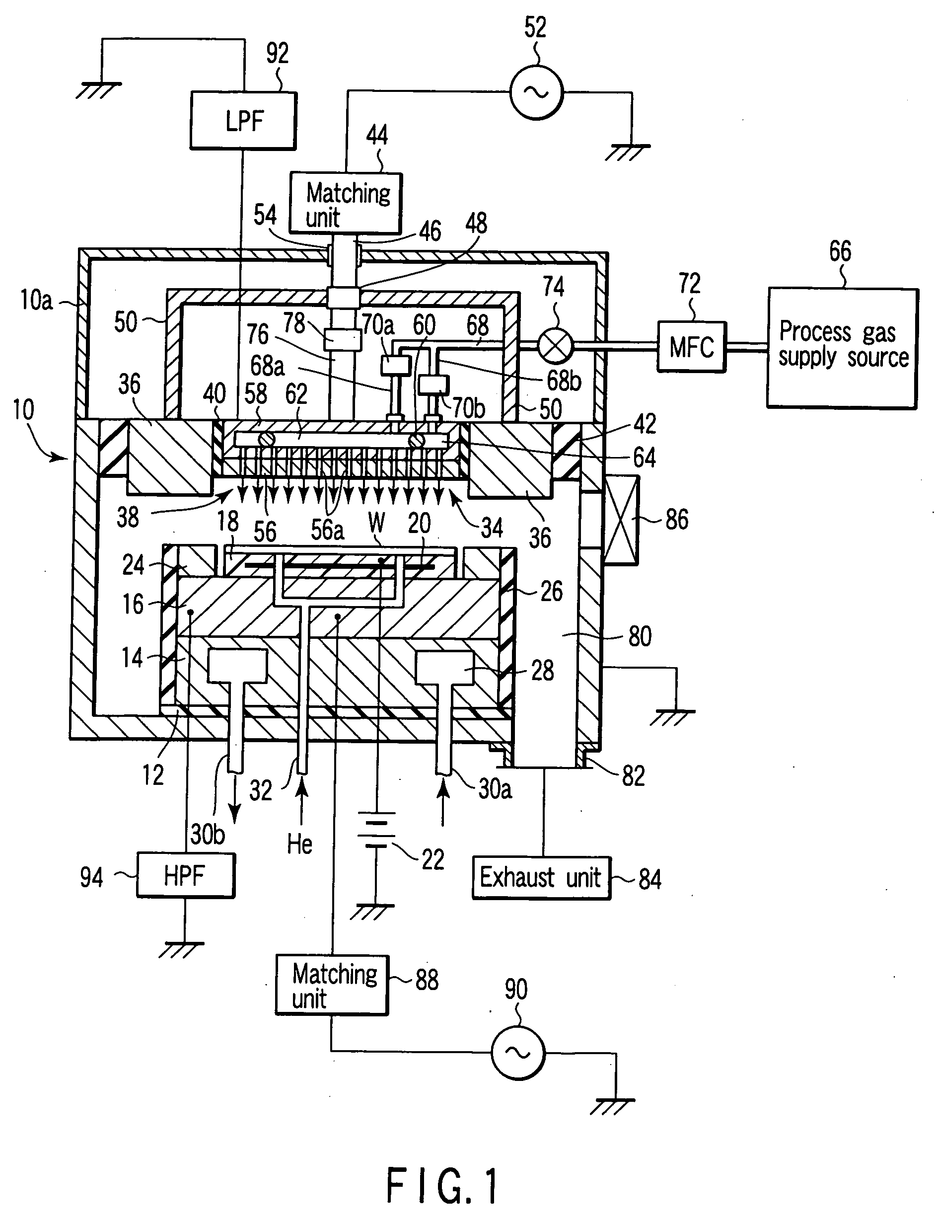
[0063]FIG. 1 is a sectional side view showing a plasma etching apparatus according to a first embodiment of the present invention. This plasma etching apparatus is structured as a parallel-plate plasma etching apparatus of the capacitive coupling type. The apparatus includes a cylindrical chamber (process container) 10, which is made of, e.g., aluminum with an alumite-processed (anodized) surface. The chamber 10 is protectively grounded.

[0064] A columnar susceptor pedestal 14 is disposed on the bottom of the chamber 10 through an insulating plate 12 made of, e.g., a ceramic. A susceptor 16 made of, e.g., aluminum is disposed on the susceptor pedestal 14. The susceptor 16 is used as a lower electrode, on which a target substrate, such as a semiconductor wafer W, is placed.

[0065] The susceptor 16 is provided with an electrostatic chuck 18 on the top, for holding the semiconductor wafer W by an electrostatic attraction force. The electrostatic chuck 18 comprises an electrode 20 made ...

second embodiment

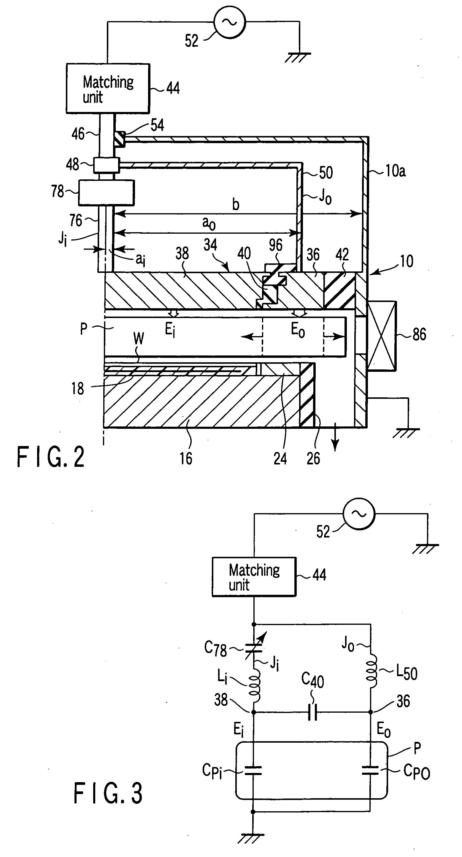
[0114]FIG. 8 is a sectional side view showing a plasma etching apparatus according to a second embodiment of the present invention. In FIG. 8, the constituent elements having substantially the same arrangement and function as those of the apparatus according to the first embodiment (FIG. 1) are denoted by the same reference numerals.

[0115] One of the features of the second embodiment resides in that the feed cylinder 50 or transmission path for transmitting the RF from the RF power supply 52 to the outer upper electrode 36 is made of a cast metal. This cast metal is preferably a metal having a high conductivity and workability, such as aluminum. As one of the advantages, cast metals can realize a low cost, and thus reduce the cost for the member to 1 / 7 or less of that provided by a plate material. As another advantage, cast metals can be easily integrated, and thus can reduce the number of RF connection surfaces in the member, thereby reducing the RF loss.

[0116] Further, even wher...

third embodiment

[0143]FIG. 21 is a sectional side view showing a main part of a plasma etching apparatus according to a third embodiment of the present invention. The parts of this apparatus can be the same as those of the second embodiment except for the featuring parts. The third embodiment has a feature in that a shield member 104 is disposed along the protrusion part 36B of the outer upper electrode 36 according to the second embodiment.

[0144] For example, the shield member 104 is formed of an aluminum plate with an alumite-processed surface, and physically and electrically coupled to the sidewall of the process container 10. The shield member 104 extends essentially in the horizontal direction from the container sidewall to the position below the protrusion part 36B of the outer upper electrode 36 to cover the bottom surfaces of the protrusion part 36B and the ring-shaped shield member 42 in a non-contacting or insulated state. The second electrode member 36B of the outer upper electrode 36 h...


PUM

PropertyMeasurementUnit
frequencyaaaaaaaaaa
frequencyaaaaaaaaaa
frequencyaaaaaaaaaa

Abstract

A plasma processing method is arranged to supply a predetermined process gas into a plasma generation space in which a target substrate is placed, and turn the process gas into plasma. The substrate is subjected to a predetermined plasma process by this plasma. The spatial distribution of density of the plasma and the spatial distribution of density of radicals in the plasma are controlled independently of each other relative to the substrate by a facing portion opposite the substrate to form a predetermined process state over the entire target surface of the substrate.

Description

CROSS REFERENCE TO RELATED APPLICATIONS [0001] This is a Continuation Application of PCT Application No. PCT / JP03 / 15029, filed Nov. 25, 2003, which was published under PCT Article 21(2) in Japanese. [0002] This application is based upon and claims the benefit of priority from prior Japanese Patent Applications No. 2002-341949, filed Nov. 26, 2002; and No. 2003-358432, filed Oct. 17, 2003, the entire contents of both of which are incorporated herein by reference.BACKGROUND OF THE INVENTION [0003] 1. Field of the Invention [0004] The present invention relates to a technique for subjecting a target substrate to a plasma process, and specifically to a plasma processing technique for processing a substrate, using radicals and ions derived from plasma. Particularly, the present invention relates to a plasma processing technique utilized in a semiconductor process for manufacturing semiconductor devices. The term “semiconductor process” used herein includes various kinds of processes which...

Claims


Application Information

Patent Timeline
Patent Type & Authority Applications(United States)
IPC IPC(8): C23F1/00B08B7/00H05H1/46C23F4/00H01J37/32H01L21/304H01L21/3065
CPCH01J37/32082H01J37/32935H01J37/32422H01L21/3065
Inventor KOSHIISHI, AKIRAHIROSE, JUNOGASAWARA, MASAHIROHIRANO, TAICHISASAKI, HIROMITSUYOSHIDA, TETSUOSAITO, MICHISHIGEISHIHARA, HIROYUKIOOYABU, JUNNUMATA, KOHJI
Owner TOKYO ELECTRON LTD
Why Eureka
Try Eureka