
Lateral semiconductor device using trench structure and method of manufacturing the same

a semiconductor device and trench structure technology, applied in the direction of semiconductor devices, basic electric elements, electrical equipment, etc., can solve the problems of prior art and hinder the improvement of driving performance, and the mounting of integrated circuit standard elements on chips with integrated circuit standard elements, so as to reduce the resistance of transistors and contact area

Active Publication Date: 2006-01-05
ABLIC INC
View PDF9 Cites 17 Cited by
  • Summary
  • Abstract
  • Description
  • Claims
  • Application Information

AI Technical Summary

Benefits of technology

The present invention provides a lateral MOS transistor with high driving performance without increasing a planar element area. The transistor has a long gate width per unit plane area and includes a gate electrode formed on trenches whose lengthwise direction is parallel to gate length direction. The transistor also has a concave portion with trenches and a second conductivity type well region formed in at least one of the trenches. The transistor has a reduced ON resistance and increased contact area between the source and drain regions, resulting in improved performance.

Problems solved by technology

However, it is also a fact that the reduction of a withstand voltage, which is caused by miniaturization of the semiconductor element, hinders further improvement of the driving performance.
The transistor shows extremely excellent performance as a single element, but has a disadvantage in mounting on a chip with standard elements for integrated circuit since the trench gate MOS transistor has a vertical MOS structure in which current flows in a depth direction of a substrate.
However, the prior art has two problems.
However, this method also has limitation on the length, and additionally, has a risk such as the reduction in concentration of the source region 001 or the drain region 002, which is caused by the excessive impurity diffusion.
This method is, therefore difficult to be actually performed.
That is, it is difficult to increase contact area in the prior art without changing the element area to reduce the ON resistance of the MOS transistor.
(2) The second problem is that there is a limitation to the trench depth.

Method used


Image

  • Lateral semiconductor device using trench structure and method of manufacturing the same
  • Lateral semiconductor device using trench structure and method of manufacturing the same
  • Lateral semiconductor device using trench structure and method of manufacturing the same

Examples


embodiment 1

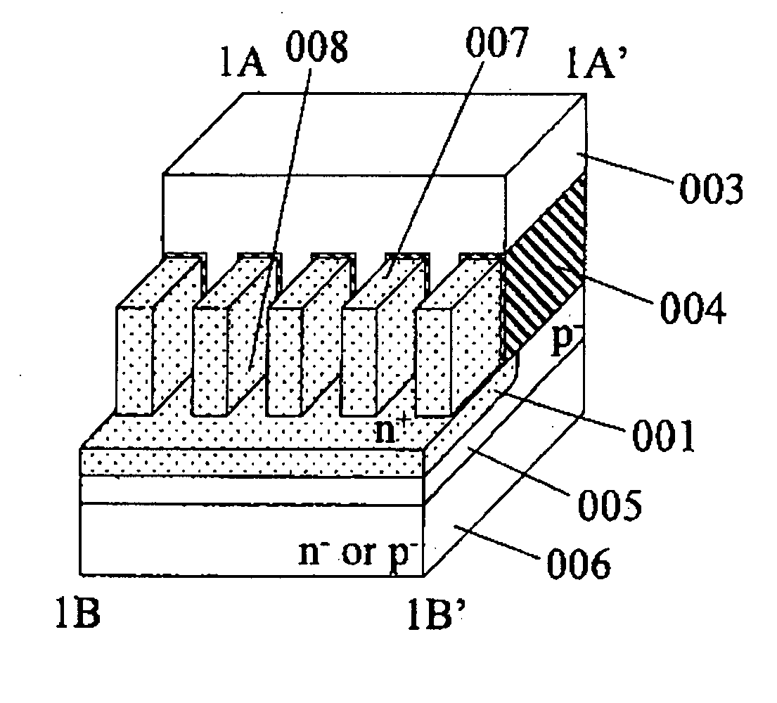
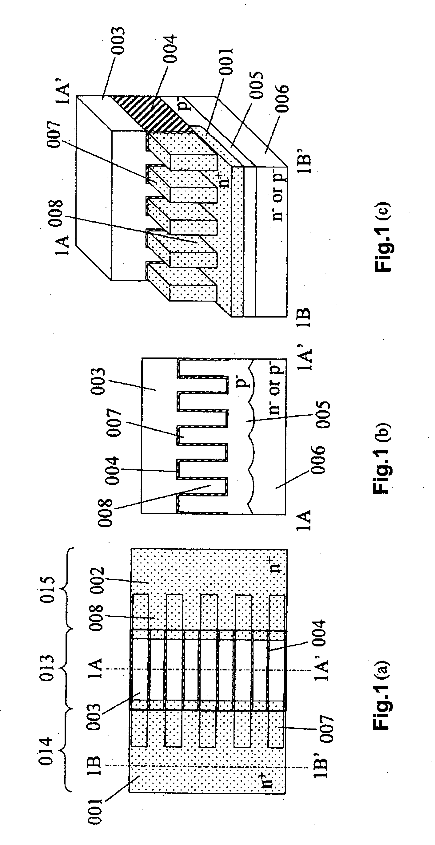
[0025]FIGS. 1A to 1C show a typical embodiment of the present invention. Here, FIG. 1A is a plan view, FIG. 1B is a sectional view taken along the line 1A-1A′ of FIG. 1A, and FIG. 1C is a perspective view cut along the line 1A-1A′ and the line 1B-1B′ of FIG. 1A. Here, in FIG. 1A, a gate electrode 003 and a gate insulating film 004 on trenches are transparent so as to be viewed easily. A bold line indicates an edge of the gate electrode 003. Further, FIG. 1C is a view seen from a source region 001. In this drawing no metal interconnect is omitted in order to show source and drain structure in three-dimensionally. This figure shows a symmetrical structure with the line 1A-1A′ as its center. Thus, the view seen from a drain region 002 is same as FIG. 1C. Note that the symmetrical structure is taken for easy understanding in the explanation of the embodiment of the present invention; however, the symmetry is not necessary in implementing the present invention.

[0026] Hereinafter, descri...

embodiment 2

[0037]FIG. 5 shows an embodiment of the present invention, which has a DDD structure. A different point of Embodiment 2 from that in Embodiment 1 is that only the third trench region 15 is opened before the formation of the source region 001 and the drain region 002, and a low level diffusion region 011 is formed which includes the drain region 002 formed in the subsequent step. Therefore, a high-driving performance MOS transistor with a high withstand voltage and a low ON resistance is completed.

embodiment 3

[0038]FIG. 6 shows an embodiment of the present invention, which has an LDMOS structure. A different point of Embodiment 3 from that in Embodiment 1 is that only the second trench region 14 is opened before the formation of the source region 001 and the drain region 002, and a body region 012 is formed which does not include the drain region 002 which are formed in the subsequent step but increases the source region 001. Therefore, a high-driving performance MOS transistor with a high withstand voltage and a low ON resistance is completed.

[0039] Described above is the embodiment of the present invention which includes the NMOS transistor in which a first conductivity type is N-type and a second conductivity type is P-type. With the use of the structure of this embodiment of the present invention, the driving performance per unit plane area can be enhanced while the same withstand voltage as that of a general planar type MOS transistor is maintained. Thus, the bottom surface of the ...


PUM


Abstract

A lateral trench MOS transistor is provided in which trenches extending to the source and drain regions are disposed parallel to the gate length direction, agate oxide is disposed on the trenches, a well is disposed under the trench region and the source and drain regions by using oblique ion implantation, a gate electrode is disposed on the gate oxide, and source and drain regions are disposed on the same plane as a bottom surface of a concave portion of the trenches self-aligned to the gate electrode by using oblique ion implantation.

Description

BACKGROUND OF THE INVENTION [0001] 1. Field of the Invention [0002] The present invention relates to a semiconductor device including a lateral MOS transistor for which high driving performance is required and to a method of manufacturing it. [0003] 2. Description of the Related Art [0004] It has become possible to manufacture small geometry MOS transistors by using progressive fine processing technique without lowering capability. This trend also applies, without exception, to semiconductor elements, for which high driving performance is required. In order to realize the high driving performance, reduction of an ON resistance of the element per unit plane area has been attempted with the best use of a fine processing technique. However, it is also a fact that the reduction of a withstand voltage, which is caused by miniaturization of the semiconductor element, hinders further improvement of the driving performance. Semiconductor devices with various structures have been proposed in...

Claims


Application Information

Patent Timeline
Patent Type & Authority Applications(United States)
IPC IPC(8): H01L29/76
CPCH01L21/26586H01L29/0657H01L29/1037H01L29/1095H01L29/7851H01L29/66795H01L29/7825H01L29/7835H01L29/4236H01L29/0847H01L29/785
Inventor RISAKI, TOMOMITSU
Owner ABLIC INC
Learn More