Novel underlayer for high performance magnetic tunneling junction MRAM

a magnetic tunneling junction and underlayer technology, applied in the field of high-performance magnetic tunneling junction elements, can solve the problems of low resistivity, high sensitive growth of ta layers and nicr/nifecr layers to starting surface conditions, inconsistent device performance, etc., and achieve the effect of high resistivity

Active Publication Date: 2006-01-05
APPLIED SPINTRONICS +1
View PDF15 Cites 87 Cited by
  • Summary
  • Abstract
  • Description
  • Claims
  • Application Information

AI Technical Summary

Benefits of technology

[0016] One objective of the present invention is to provide a capping layer for the bottom electrode of an MRAM cell or for the bottom lead (S1) in a TMR read head that promotes consistent growth of a subsequently formed MTJ element, has a high resistivity, and does not require a heavy preclean before MTJ deposition.
[0017] A further objective of the present invention is to provide an amorphous seed layer in an MTJ element that consistently enables the smooth and densely packed growth of subsequent layers including an AFM layer, a pinned layer, and a tunnel barrier layer.

Problems solved by technology

However, the growth of a Ta layer and NiCr / NiFeCr layer are highly sensitive to starting surface conditions.
However, depending on the Ta structure, NiCr or NiFeCr seed layer growth on a Ta layer is sometimes inconsistent which leads to inconsistent device performance.
Unfortunately, in the case of the commonly used NiCr / Ru / Ta bottom electrode configuration, the Ta layer is grown with a low resistivity α-structure.
The highly conductive redeposited Ta material tends to shunt a sense current around the tunneling barrier in the MTJ element 1 and causes a major device issue.
However, the '336 patent does not disclose whether the TaN is amorphous or crystalline and teaches that a seed layer such as Au, Pt, Ta, Ti, or Cr is needed to control crystal orientation and crystallinity in the MTJ stack.
However, the '220 patent does not teach that the TaN layer must be amorphous or provide a method of forming the TaN layer.

Method used


Image

  • Novel underlayer for high performance magnetic tunneling junction MRAM
  • Novel underlayer for high performance magnetic tunneling junction MRAM
  • Novel underlayer for high performance magnetic tunneling junction MRAM

Examples


first embodiment

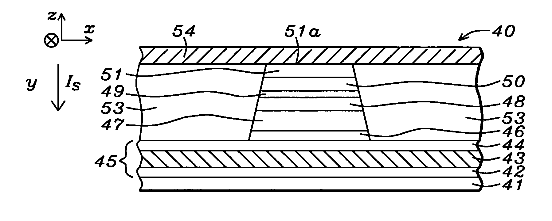
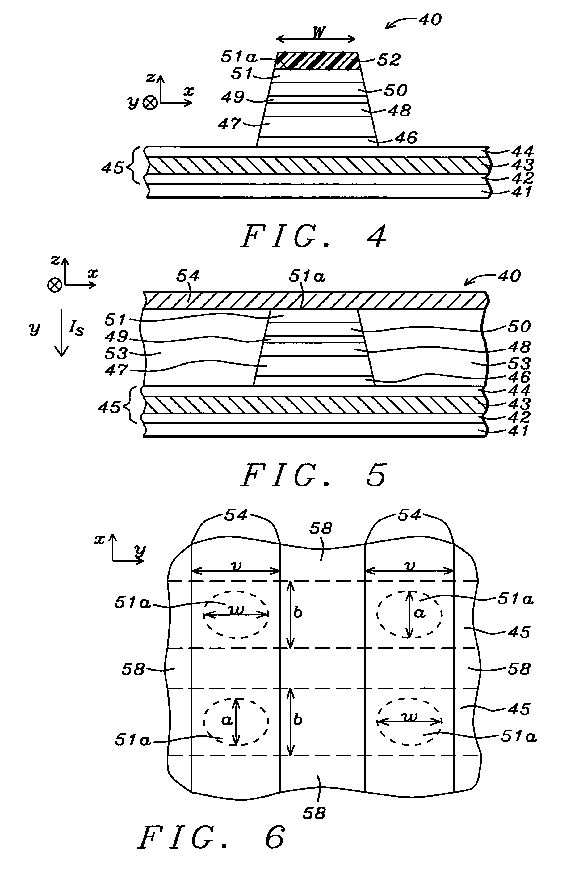
[0034] An MRAM structure formed according to the present invention will now be described. Referring to FIG. 4, a partially completed MRAM structure 40 is shown that includes a substrate 41 which may be silicon or another semiconductor substrate used in the art that typically contains other structures and devices such as transistors and diodes. A bottom electrode 45 which is a composite layer having a seed layer / conductive layer / capping layer configuration is formed on the substrate 41 and is typically coplanar with an insulation layer (not shown).

[0035] It is understood that the MRAM structure is part of an MRAM array in which multiple bottom electrodes are formed in a first conductive layer and multiple top electrodes such as parallel bit lines or word lines are formed in a second conductive layer above the bottom electrodes. An MTJ element is formed between a first and second conductive layer at each location where a top electrode crosses over a bottom electrode. The bottom electr...

second embodiment

[0050] Referring to FIG. 7, the bottom electrode 55 is comprised of a seed layer 42 and an overlying conductive layer 43. The seed layer 42 and conductive layer 43 have a thickness and composition as previously described. For example, the bottom electrode 55 may have a NiCr / Ru, NiCr / Cu, or a Ta / Cu configuration. It should be noted that a Ru or Cu surface is easier to clean than a conventional Ta capping layer on a bottom electrode. Other bottom electrode configurations that include a capping layer are acceptable although a capping layer for the bottom electrode is not necessary in this embodiment. The second embodiment affords a greater flexibility in selecting a bottom electrode composition because the subsequently formed α-TaN seed layer isolates the MTJ stack from the influence of the bottom electrode 55.

[0051] An MTJ stack of layers is disposed on the bottom electrode 55 by sequentially forming a seed layer 56, AFM layer 47, SyAP pinned layer 48, tunnel barrier layer 49, free la...

third embodiment

[0054] In a third embodiment depicted in FIG. 8, a magnetoresistive (MR) read head 60 hereafter referred to as a TMR read head is shown in which an MTJ element is formed between a bottom shield (S1) 65 and a top shield (S2) 75. An α-TaN layer is incorporated as a capping layer in the bottom shield. Although the MTJ element in the exemplary embodiment has a bottom spin valve configuration, the present invention also applies to an MTJ element with a top spin valve structure.

[0055] A substrate 61 is provided that may be AlTiC, for example. An important feature is that a bottom shield 65 which is a composite layer having a NiFe / α-TaN configuration is formed on the substrate 61. The main portion of the bottom shield 65 is a magnetic layer 62 comprised of NiFe with a thickness of about 2 microns. There is an α-TaN capping layer 64 with a thickness of about 50 to 400 Angstroms formed on the magnetic layer 62 by a previously described method. The α-TaN capping layer is employed to promote a...


PUM


Abstract

An MRAM structure is disclosed in which the bottom electrode has an amorphous TaN capping layer to consistently provide smooth and dense growth for AFM, pinned, tunnel barrier, and free layers in an overlying MTJ. Unlike a conventional Ta capping layer, TaN is oxidation resistant and has high resistivity to avoid shunting of a sense current caused by redeposition of the capping layer on the sidewalls of the tunnel barrier layer. Alternatively, the α-TaN layer is the seed layer in the MTJ. Furthermore, the seed layer may be a composite layer comprised of a NiCr, NiFe, or NiFeCr layer on the α-TaN layer. An α-TaN capping layer or seed layer can also be used in a TMR read head. An MTJ formed on an α-TaN capping layer has a high MR ratio, high Vb, and a RA similar to results obtained from MTJs based on an optimized Ta capping layer.

Description

RELATED PATENT APPLICATIONS [0001] This application is related to the following: Docket # HT03-022, Ser. No. 10 / 844,171, filing date May 12, 2004; and Docket # HT03-025 / 031, Ser. No. 10 / 849,310, filing date May 19, 2004; all assigned to a common assignee.FIELD OF THE INVENTION [0002] The invention relates to a high performance Magnetic Tunneling Junction (MTJ) element and a method for making the same, and more particularly, to a seed layer for the MTJ element that can also serve as the capping layer for a bottom electrode in an MRAM device. BACKGROUND OF THE INVENTION [0003] A magnetic random access memory (MRAM) device is generally comprised of a cross point design in which an array of parallel second conductive lines crosses over an array of parallel first conductive lines, and an MTJ element is formed between a first conductive line and second conductive line at each crossover point. A first conductive line may be a word line while a second conductive line is a bit line or vice v...

Claims


Application Information

Patent Timeline
Patent Type & Authority Applications(United States)
IPC IPC(8): G11C11/14
CPCB82Y10/00H01F10/3259B82Y40/00G01R33/09G01R33/093G01R33/098G11B5/3906G11B5/3909G11C11/15G11C11/16H01F10/30H01F10/3254H01F10/3272H01F41/307H01L43/10H01L43/12Y10T428/1114H01F10/3295B82Y25/00G11C11/161G11C11/1673H10B61/00H10N50/01H10N50/85H10N50/10
Inventor HONG, LIUBOHORNG, CHENGCHEN, MAO-MINTONG, RU-YIN
Owner APPLIED SPINTRONICS
Why Eureka
Try Eureka