Ultrathin chemically grown oxide film as a dopant diffusion barrier in semiconductor devices

a technology of chemical growth and diffusion barrier, which is applied in the direction of digital storage, semiconductor/solid-state device details, instruments, etc., can solve the problems of difficult to maintain sharp transitions in doping profiles, dopants that cannot reliably remain where they're, and dopants that tend to diffus

Inactive Publication Date: 2006-01-12
SANDISK TECH LLC
View PDF1 Cites 79 Cited by
  • Summary
  • Abstract
  • Description
  • Claims
  • Application Information

AI Technical Summary

Benefits of technology

[0008] A first aspect of the invention provides for a semiconductor device in an integrated circuit comprising: a first semiconductor layer; a chemically grown oxide grown on the first semiconductor layer, wherein the chemically grown oxide comprises nitrogen and is no more than about 7 angstroms thick; and a second semiconductor layer in immediate contact with the chemically grown oxide, wherein the first semiconductor layer or the second semiconductor layer is doped with a first conductivity-enhancing dopant, and wherein, after fabrication of the integrated circuit is complete, a concentration of the first conductivity-enhancing dopant is at least ten times higher in one of the first semiconductor or the second semiconductor layer than in the other of the first semiconductor layer or the second semiconductor layer.
[0009] Another aspect of the invention provides for a method for forming a semiconductor device, the method comprising: forming a first semiconductor layer; growing a chemically grown oxide on the first semiconductor layer in a liquid ambient; forming a second semiconductor layer directly on the chemically grown oxide, wherein the first semiconductor layer or the second semiconductor layer is doped with a first conductivity-enhancing dopant; and subjecting the first semiconductor layer, the chemically grown oxide layer, and the second semiconductor layer to a temperature exceeding about 700 degrees C., wherein the chemically grown oxide inhibits diffusion of the first conductivity-enhancing dopant between the first and second semiconductor layers.

Problems solved by technology

Dopants do not reliably remain where they've been placed through implantation or in situ doping, however.
Dopants tend to diffuse, and, particularly in smaller devices, sharp transitions in doping profiles can be difficult to maintain.
Barriers can be used to prevent dopant diffusion, but in general such barriers will significantly change the electrical properties of the device.

Method used


Image

  • Ultrathin chemically grown oxide film as a dopant diffusion barrier in semiconductor devices
  • Ultrathin chemically grown oxide film as a dopant diffusion barrier in semiconductor devices
  • Ultrathin chemically grown oxide film as a dopant diffusion barrier in semiconductor devices

Examples


Embodiment Construction

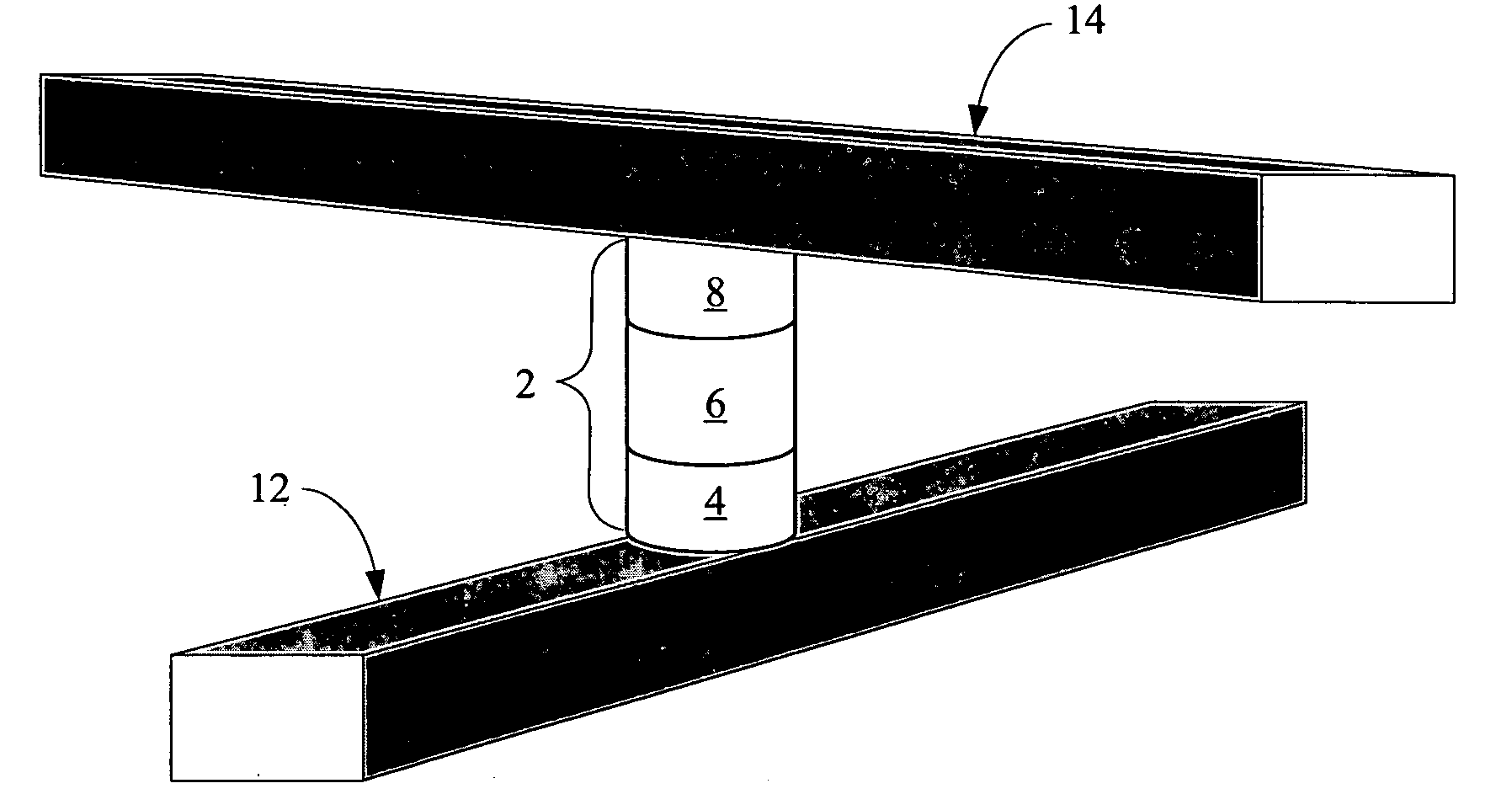
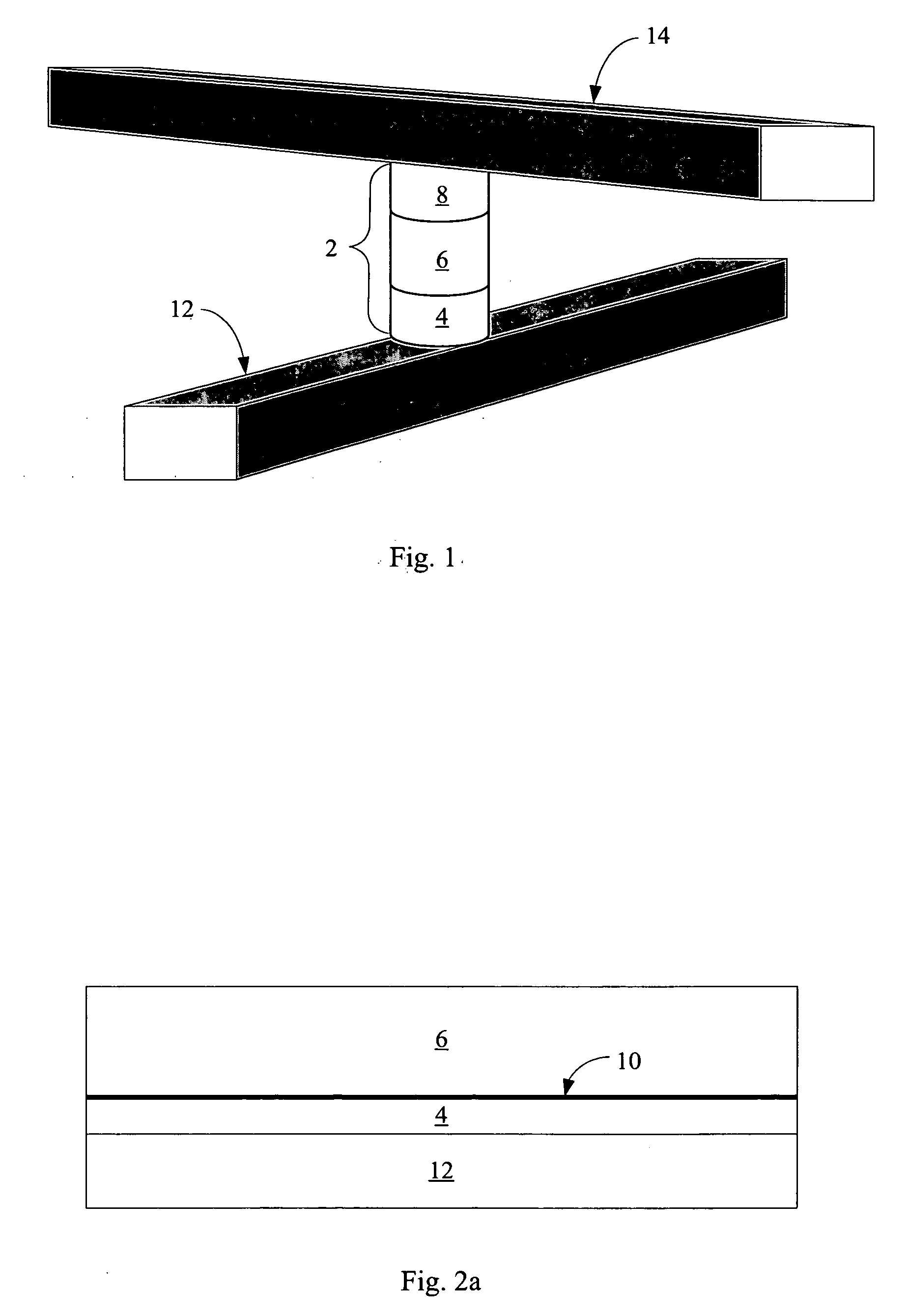
[0007] The present invention is defined by the following claims, and nothing in this section should be taken as a limitation on those claims. In general, the invention is directed to a chemically grown oxide film that serves as a dopant diffusion barrier.

[0008] A first aspect of the invention provides for a semiconductor device in an integrated circuit comprising: a first semiconductor layer; a chemically grown oxide grown on the first semiconductor layer, wherein the chemically grown oxide comprises nitrogen and is no more than about 7 angstroms thick; and a second semiconductor layer in immediate contact with the chemically grown oxide, wherein the first semiconductor layer or the second semiconductor layer is doped with a first conductivity-enhancing dopant, and wherein, after fabrication of the integrated circuit is complete, a concentration of the first conductivity-enhancing dopant is at least ten times higher in one of the first semiconductor or the second semiconductor laye...


PUM


Abstract

The invention is a chemically grown oxide layer which prevents dopant diffusion between semiconductor layers. The chemically grown oxide layer may be so thin that it does not form a barrier to electrical conduction, and thus may be formed within active devices such as diodes or bipolar transistors. Such a chemically grown oxide film is advantageously used to prevent dopant diffusion in a vertically oriented polysilicon diode formed in a monolithic three dimensional memory array.

Description

RELATED APPLICATIONS [0001] This application is a continuation-in-part of Herner et al., U.S. patent application Ser. No. 11 / 015,824, “Nonvolatile Memory Cell Comprising a Reduced Height Vertical Diode,” filed Dec. 17, 2004 and hereinafter the '824 application, which is a continuation-in-part of Herner, U.S. patent application Ser. No. 10 / 955,549, “Nonvolatile Memory Cell Without a Dielectric Antifuse Having High- and Low-Impedance States,” filed Sep. 29, 2004, hereinafter the '549 application; which is a continuation-in-part of Herner et al., U.S. patent application Ser. No. 10 / 855784, “A High-Density Three-Dimensional Memory Cell,” filed May 26, 2004; which is a continuation of Herner et al., U.S. patent application Ser. No. 10 / 326470, “An Improved Method for Making High-Density Nonvolatile Memory,” filed Dec. 19, 2002 (since abandoned) and hereinafter the '470 application, all assigned to the assignee of the present invention and hereby incorporated by reference in their entirety...

Claims


Application Information

Patent Timeline
Patent Type & Authority Applications(United States)
IPC IPC(8): H01L29/00
CPCG11C5/02H01L27/2463G11C17/06G11C17/16G11C2213/71G11C2213/77H01L27/1021H01L29/0649H01L29/66272H01L29/732H01L29/868H01L45/04H01L45/1233H01L45/146H01L27/2409G11C11/39H10B63/20H10B63/80H10N70/20H10N70/8833H10N70/826
Inventor HERNER, S. BRADECKERT, VICTORIA L.
Owner SANDISK TECH LLC
Why Eureka
Try Eureka