Plastic encapsulated semiconductor device with reliable down bonds

Inactive Publication Date: 2006-01-12
TEXAS INSTR INC
View PDF14 Cites 29 Cited by
  • Summary
  • Abstract
  • Description
  • Claims
  • Application Information

AI Technical Summary

Benefits of technology

[0012] The plastic encapsulated semiconductor device of the invention includes an integrated circuit chip interconnected by one or more reliable down bond wires to the chip pad substrate and by conventional wire bonds to the leads. The substrate comprises a chip mount pad and leads. The chip mount pad is larger than the chip, includes one or more elevated topographical features, and has one or more bondable sites on th

Problems solved by technology

A frequent reliability issue with plastic encapsulated devices is delamination, most frequently occurring at an interface between the encapsulation and the largest topographically uninterrupted surface of the lead frame or other substrate.
A variety of material, design, and environmental factors contribute to delaminating, but the failure is most pronounced at the interface between the smooth surface of the chip pad and plastic encapsulation.
Delamination is particularly worrisome in the case of a large chip pad and smaller chip.
Reliable down bonds cannot be made in regions of potential delamination because high levels of stress will be placed on the thin, fragile bond wire.
Thin devices having plastic encapsulation only on one side, such as CSP, QFN, and SON packages are particularly susceptible to delamination because of thermal stresses and substrate distortion.
Such gr

Method used


Image

  • Plastic encapsulated semiconductor device with reliable down bonds
  • Plastic encapsulated semiconductor device with reliable down bonds
  • Plastic encapsulated semiconductor device with reliable down bonds

Examples


Example

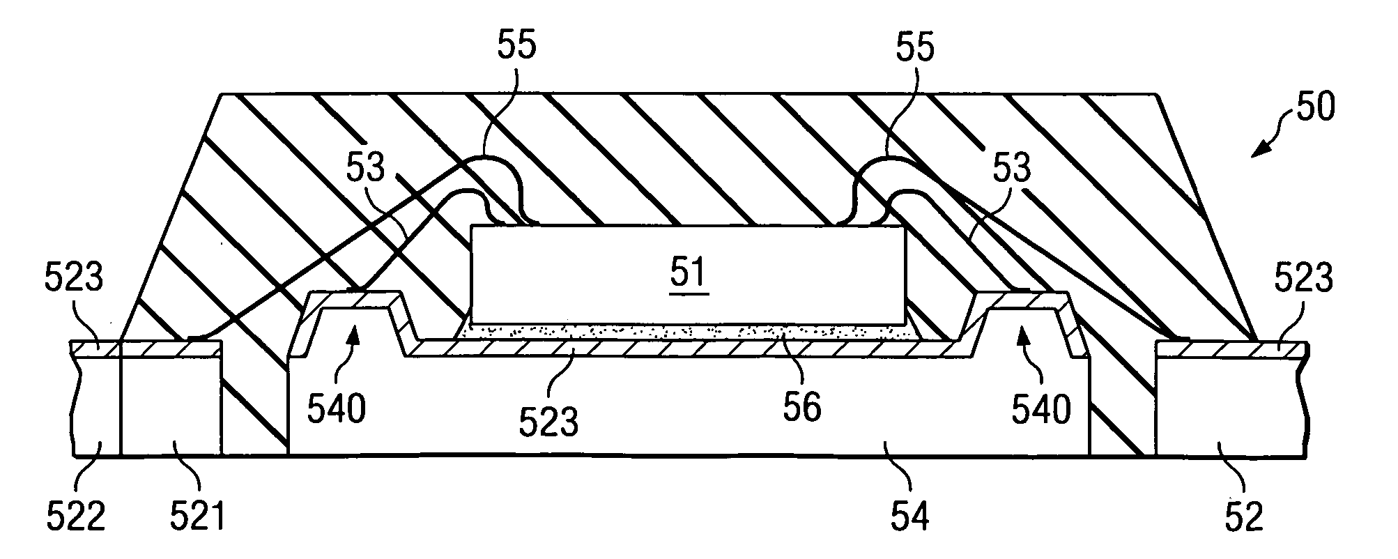
[0033]FIG. 5 illustrates in cross section a semiconductor device 50 having elevated topographical structures 540 formed on the top surface of chip mount pad 54 for the purpose of enhancing adhesion between the encapsulating plastic resin 57 and mount pad 54, thereby allowing bondable areas for reliable down bonds 53 to be provided. Down bonds of gold wires 53 are attached to bondable surfaces on the chip mount pad wherein delamination is controlled. Gold wire bonding to a substrate, known in the semiconductor industry, requires a smooth surface covered by a noble material typically gold, palladium, or silver.

[0034] Elevated structures 540 disrupt delamination of the plastic encapsulation to chip mount interface without the need for grooves or other indentations which may increase substrate distortion and further increase stresses at the interface, thus placing unacceptable high levels of stress on the wire bond. Height of the elevated structures is in the range of 5 to 25 microns a...


PUM


Abstract

Plastic encapsulated semiconductor devices having elevated topographical features on the chip mount pad to control the extent of delamination at the plastic to substrate interface, thereby allowing reliable down bond sites to be formed on the top surface of the chip mount pad which may serve as a ground plane. The cost effective invention is applicable to a variety of semiconductor packages, including both leaded and non-leaded types for high frequency circuits.

Description

FIELD OF THE INVENTION [0001] The present invention is related to a semiconductor device, and more particularly to a device having reliable down bonds. BACKGROUND OF THE INVENTION [0002] Plastic encapsulated semiconductor devices typically include an integrated circuit chip having mechanical and electrical contacts to a substrate which, in turn, provides connections to an electronic system external to the device. Substrates typically are a metallic lead frame or an insulating base having a plurality of patterned conductive leads. Ball grid array (BGA) packages and some chip scale packages (CSP) are examples of the latter substrate type. Among others, packages with lead frames include quad flat packages (QFP), small outline packages (SOP), and J-lead small outline devices (SOJ). Recently, much emphasis has been placed on circuit board space saving devices such as quad flat no lead (QFN), small outline no lead (SON), and other devices having small area of the lead contacts protruding ...

Claims


Application Information

Patent Timeline
IPC IPC(8): H01L23/02
CPCH01L23/3107H01L23/49503H01L23/49551H01L23/49582H01L24/45H01L24/49H01L2224/32245H01L2224/45144H01L2224/48091H01L2224/48137H01L2224/48247H01L2224/48257H01L2224/48472H01L2224/49171H01L2224/49175H01L2224/73265H01L2224/85464H01L2924/01028H01L2924/01029H01L2924/01042H01L2924/01046H01L2924/01047H01L2924/01075H01L2924/01078H01L2924/01079H01L2924/01082H01L2924/14H01L24/48H01L2924/01023H01L2924/01087H01L2924/014H01L2224/32257H01L24/32H01L2924/00014H01L2924/00H01L2924/351H01L2924/181H01L2224/48664H01L2924/00012
Inventor KODURI, SREENIVASAN K.
Owner TEXAS INSTR INC
Why Eureka
Try Eureka