Growth of planar, non-polar a-plane gallium nitride by hydride vapor phase epitaxy

a gallium nitride, aplane technology, applied in the direction of crystal growth process, polycrystalline material growth, chemically reactive gases, etc., can solve the problems of reducing the electron-hole recombination efficiency, red-shifting the emission wavelength, and not being able to simply cut a crystal, etc., to reduce the oxygen level and reduce the pressure of the reactor

Active Publication Date: 2006-01-12
JAPAN SCI & TECH CORP +1
View PDF33 Cites 115 Cited by
  • Summary
  • Abstract
  • Description
  • Claims
  • Application Information

AI Technical Summary

Benefits of technology

[0016] The present invention discloses a method for forming a planar, non-polar, a-plane gallium nitride (GaN) film on a substrate, comprising: (a) loading a substrate into a reactor; (b) evacuating the reactor and backfilling the reactor with purified nitrogen (N2) gas to reduce oxygen levels therein; (c) heating the reactor to a growth temperature of approximately 1040° C., with a mixture of hydrogen (H2) and nitrogen (N2) flowing through all channels in the reactor; (d) nitridating the substrate by adding anhydrous ammonia (NH3) to a gas stream in the reactor to nitridate the substrate; (e) reducing the reactor's pressure to a desired deposition pressure, wherein the desired deposition pressure is approximately 76 Torr; (f) initiating a gaseous hydrogen chloride (HCl) flow to a gallium (Ga) source to begin growth of the a-plane GaN film directly on the substrate, wherein the gaseous HCl reacts with the Ga at a temperature in excess of 600° C. to form gallium monochloride (GaCl); (g) transporting the GaCl to the substrate using a carrier gas that includes at least a fraction of hydrogen (H2), wherein the GaCl reacts with ammonia (NH3) at the substrate to form the GaN film; and (h) after a desired growth time has elapsed, interrupting the gaseous HCl flow, returning the reactor's pressure to atmospheric pressure, reducing the reactor's temperature to room temperature, and including anhydrous ammonia H3) in a gas stream to prevent decomposition of the GaN film during the reduction of the reactor's temperature.

Problems solved by technology

Charge separation within quantum wells decreases the electron-hole recombination efficiency and red-shifts the emission wavelength [4-8], both of which are undesirable in the operation of the operation of light-emitting optoelectronic devices.
Bulk crystals of GaN are not available so it is not possible to simply cut a crystal to present a surface for subsequent device regrowth.
However, to date, it has only been possible to grow planar c-plane GaN films by HVPE.
Such a surface structure is clearly unacceptable for use as either a substrate or device layer material.

Method used


Image

  • Growth of planar, non-polar a-plane gallium nitride by hydride vapor phase epitaxy
  • Growth of planar, non-polar a-plane gallium nitride by hydride vapor phase epitaxy
  • Growth of planar, non-polar a-plane gallium nitride by hydride vapor phase epitaxy

Examples


Embodiment Construction

[0026] In the following description of the preferred embodiment, reference is made to the accompanying drawings which form a part hereof, and in which is shown by way of illustration a specific embodiment in which the invention may be practiced. It is to be understood that other embodiments may be utilized and structural changes may be made without departing from the scope of the present invention.

[0027] Overview

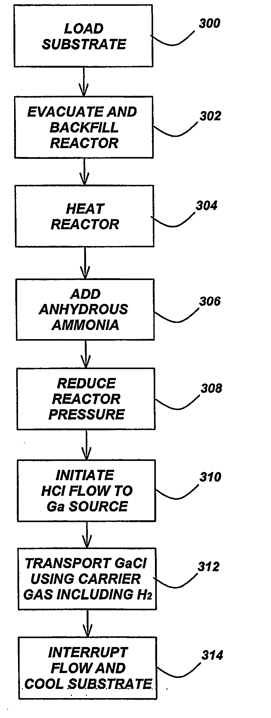
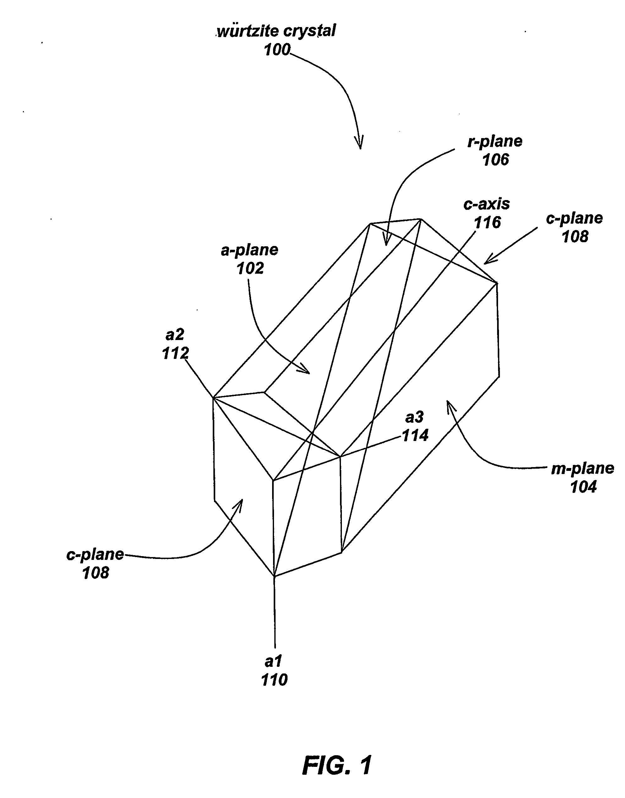
[0028] The present invention uses hydride vapor phase epitaxy (HVPE) to grow planar, non-polar, a-plane gallium nitride (GaN) films. Specifically, the present invention relies on the use of a combination of several growth parameters to achieve these planar, non-polar, a-plane gallium nitride (GaN) films: [0029] 1. The use of a suitable substrate, such as, but not limited to, an r-plane sapphire (Al2O3) substrate. [0030] 2. The use of a fraction of hydrogen (H2) as a carrier gas for the final growth stage in one or more of the gas streams in a reactor.

[0031] 3. A reduced r...


PUM


Abstract

Highly planar non-polar a-plane GaN films are grown by hydride vapor phase epitaxy (HVPE). The resulting films are suitable for subsequent device regrowth by a variety of growth techniques

Description

CROSS-REFERENCE TO RELATED APPLICATIONS [0001] This application claims priority to the following co-pending and commonly-assigned U.S. Provisional Patent Applications: [0002] Ser. No. 60 / 433,844, entitled “TECHNIQUE FOR THE GROWTH OF PLANAR, NON-POLAR A-PLANE GALLIUM NITRIDE BY HYDRIDE VAPOR PHASE EPITAXY,” filed on Dec. 16, 2002, by Benjamin A. Haskell, Paul T. Fini, Shigemasa Matsuda, Michael D. Craven, Steven P. DenBaars, James S. Speck, and Shuji Nakamura, attorneys docket number 30794.94-US-P1; and [0003] Ser. No. 60 / 433,843, entitled “GROWTH OF REDUCED DISLOCATION DENSITY NON-POLAR GALLIUM NITRIDE BY HYDRIDE VAPOR PHASE EPITAXY,” filed on Dec. 16, 2002, by Benjamin A. Haskell, Michael D. Craven, Paul T. Fini, Steven P. DenBaars, James S. Speck, and Shuji Nakamura, attorneys docket number 30794.93-US-P1; [0004] both of which applications are incorporated by reference herein. [0005] This application is related to co-pending and commonly-assigned International Application No. PCT...

Claims


Application Information

Patent Timeline
Patent Type & Authority Applications(United States)
IPC IPC(8): H01L21/00
CPCC30B25/02C30B29/40C30B29/406H01L21/02389H01L21/0262H01L21/02433H01L21/0254H01L21/02587H01L21/02609H01L21/0242
Inventor HASKELL, BENJAMIN A.FINI, PAUL T.MATSUDA, SHIGEMASACRAVEN, MICHAEL D.DENBAARS, STEVEN P.SPECK, JAMES S.NAKAMURA, SHUJI
Owner JAPAN SCI & TECH CORP
Why Eureka
Try Eureka