Method for forming insulating film on substrate, method for manufacturing semiconductor device and substrate-processing apparatus

Inactive Publication Date: 2006-01-12
TOKYO ELECTRON LTD
View PDF4 Cites 245 Cited by
  • Summary
  • Abstract
  • Description
  • Claims
  • Application Information

AI Technical Summary

Benefits of technology

[0040] In accordance with the method for forming the insulating film, the method for manufacturing the semiconductor device and the apparatus for processing the substrate based on the aforementioned substrate processing technique, the nitrogen radicals and the oxygen radicals excited through the high frequency plasma can form an extremely thin oxynitride film in a one step process. Accordingly, the productivity is improved through a reduction in the number of steps required over the prior art technique wherein the nitriding of the oxide film is

Problems solved by technology

However, such an extremely thin gate insulating film cannot avoid the problem of increased gate leakage current resulting from an increase in the tunneling current.
The base oxide film needs to be very thin since the merit of employing the high-k dielectric film as a gate insulating film might be lost otherwise.
Problem arises with such heat treatment on the high-k dielectric film 13 due to the increase in the film thickness of the base oxide film 12.
Such an increase in the film thickness of the base oxide film 12 poses a very serious problem especially when the film thickness of the base oxide film 12 needs to be reduced to a level equivale

Method used


Image

  • Method for forming insulating film on substrate, method for manufacturing semiconductor device and substrate-processing apparatus
  • Method for forming insulating film on substrate, method for manufacturing semiconductor device and substrate-processing apparatus
  • Method for forming insulating film on substrate, method for manufacturing semiconductor device and substrate-processing apparatus

Examples


Embodiment Construction

[0059] The preferred embodiment of the present invention will now be explained with reference to the drawings.

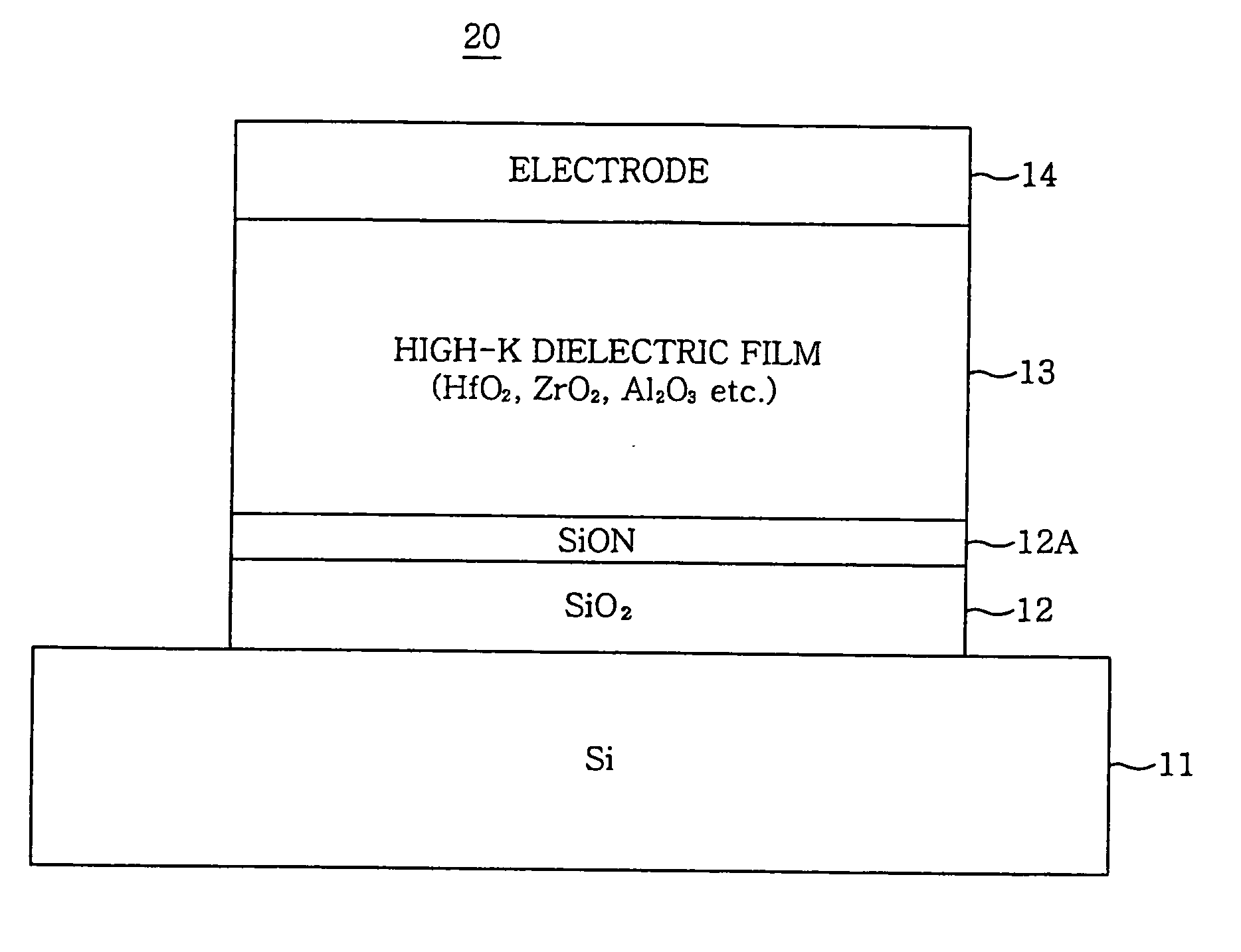
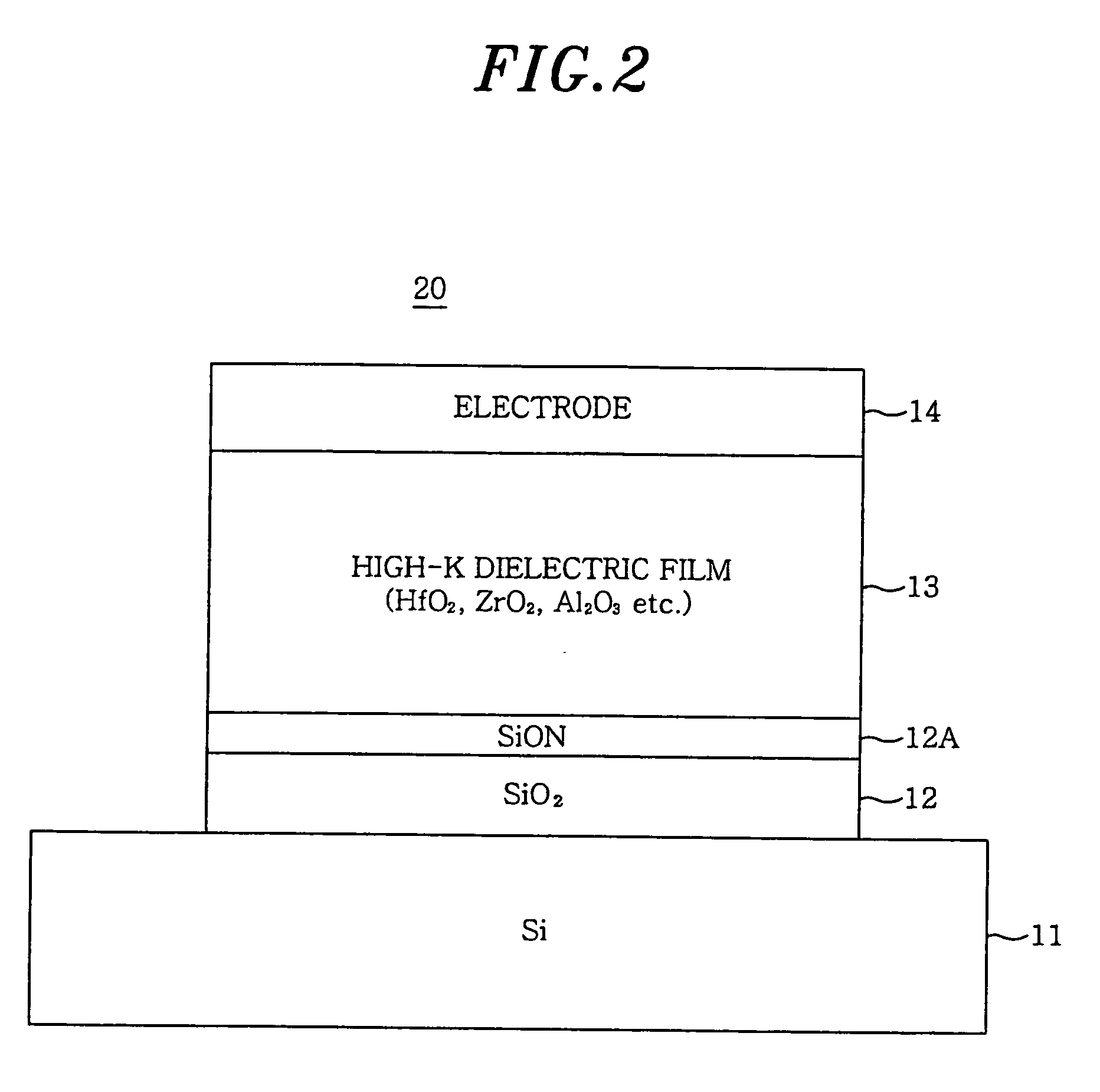
[0060]FIG. 3 shows a sketchy diagram of an apparatus 100 for processing a substrate in accordance with the preferred embodiment of the present invention. Through the use of such apparatus 100, an oxynitride film is formed on the silicon wafer 11 as shown in FIG. 2.

[0061] The apparatus 100 for processing the substrate includes a processing vessel 21, a remote plasma source 26 for producing nitrogen radicals and oxygen radicals using a high frequency plasma and a gas supply unit 30 for feeding a raw gas into the remote plasma source 26.

[0062] The processing vessel 21 accommodates a substrate supporting table 22 with a heater 22A attached thereto. The substrate supporting table 22 moves between a wafer loading / unloading position and a process position in a vertical way. A drive mechanism 22C rotates the substrate supporting table 22. The inner wall of the processing vessel 2...


PUM

PropertyMeasurementUnit
Ratioaaaaaaaaaa
Frequencyaaaaaaaaaa

Abstract

A substrate-processing apparatus (100, 40) comprises a radical-forming unit (26) for forming the nitrogen radicals and oxygen radicals through a high-frequency plasma, a processing vessel (21) in which a substrate (W) to be processed is held, and a gas-supplying unit (30) which is connected to the radical-forming unit. The gas-supplying unit (30) controls the mixture ratio between a first raw material gas containing the nitrogen and a second raw material gas containing oxygen, and supplies a mixture gas of a desired mixture ratio to the radical-forming unit. By supplying the nitrogen radicals and oxygen radicals mixed at the controlled mixture ratio to the surface of the substrate, an insulating film having a desired nitrogen concentration is formed on the surface of the substrate.

Description

FIELD OF THE INVENTION [0001] The present invention relates to a method for manufacturing a semiconductor device; and, more particularly, to a substrate processing technique of a super miniaturized high speed semiconductor device wherein a high-k dielectric film is employed as a gate insulating film. BACKGROUND OF THE INVENTION [0002] With the advancement in the miniaturization process technology, it has become feasible to use a gate length of 0.1 μm or less in an ultra high speed semiconductor device. Generally, the operating speed of a semiconductor device is improved with the miniaturization thereof. However, in such a highly miniaturized semiconductor device, the thickness of a gate insulating film needs to be reduced in proportion to the reduction in the gate length in accordance with the scaling rule. [0003] In case the gate length is reduced to 0.1 μm or less, the thickness of the gate insulating film needs to be 1-2 nm or less on a conventional thermal oxide film basis. Howe...

Claims


Application Information

Patent Timeline
IPC IPC(8): C23C16/00H01L21/31H01L21/00H01L21/314H01L21/318H01L29/78
CPCH01L21/67017H01L21/3144H01L21/02274H01L21/0228H01L21/02142H01L21/02164H01L21/02225
Inventor IGETA, MASANOBUAOYAMA, SHINTAROSHINRIKI, HIROSHI
Owner TOKYO ELECTRON LTD
Why Eureka
Try Eureka